DE10-Nano: HPS loan I/O example
Introduction
I've made a mistake on my older revision page regarding the loan I/O not being a direct connection. The pin multiplexor is physically routing the dedicated HPS pins to the FPGA. Moving forward, let's see how to get the loan I/O working with the serial UART.
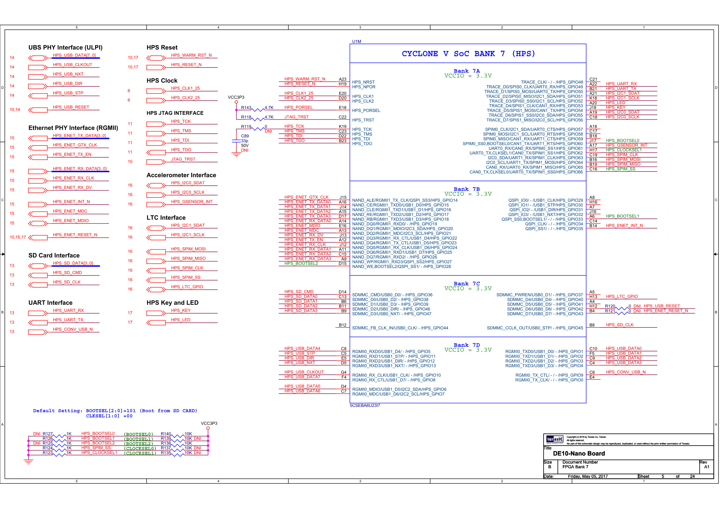
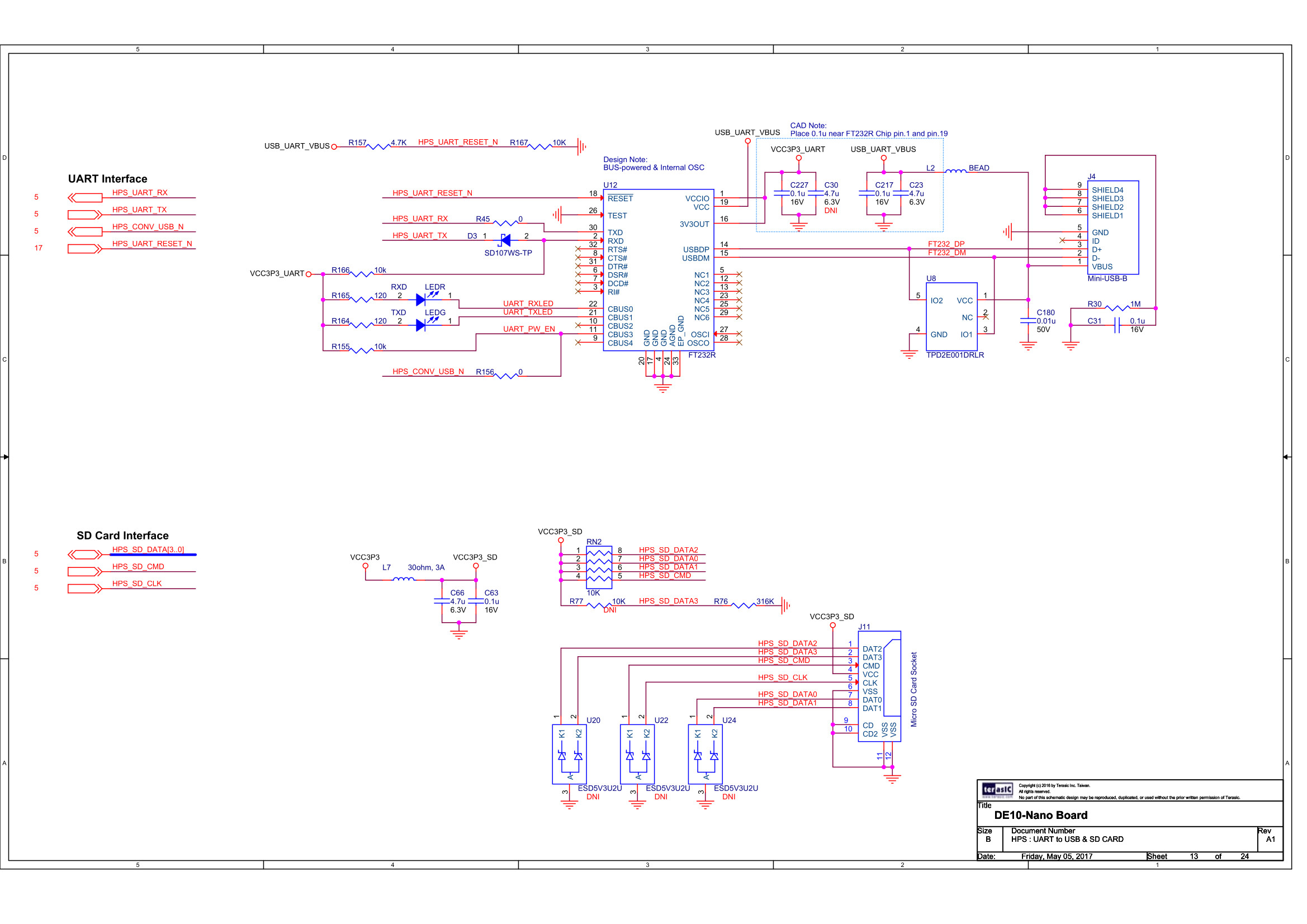
On the DE10-Nano board, the mini-B USB is connected to a USB to serial UART IC (FTDI FT232R) for HPS side. From the schematics we can see the following connections:
| Net name | Hardware pin | Cyclone V SoC pin (HPS) |
|---|---|---|
| HPS_UART_RX | Pin 30 (FT232R TXD) | Pin A22 (HPS_UART0_RX/HPS_GPIO49/HPS_LOANIO49) |
| HPS_UART_TX | Pin 2 (FT232R RXD) | Pin B21 (HPS_UART0_TX/HPS_GPIO50/HPS_LOANIO50) |
| HPS_LED | Anode pin (HPS user LED) | Pin A20 (HPS_GPIO53/HPS_LOANIO53) |
Basically, we would like to control these pins from the FPGA:
- LoanIO 49 = input serial from UART rx line
- LoanIO 50 = output serial to UART tx line
- LoanIO 53 = output level to LED
Schematic of Cyclone V SoC bank 7 section:
Schematic of UART-USB section:
Reusing an existing Quartus project
To save time, let's use an existing Quartus project instead of starting from scratch. We can start by making a copy of my f2h_uart_de10nano project. We need to change the project name with these steps:
Rename files:
- Rename f2h_uart_tx.qpf file to loanio_uart_tx.qpf
- Rename f2h_uart_tx.qsf file to loanio_uart_tx.qsf
- Rename f2h_uart_tx.qws file to loanio_uart_tx.qws
- Rename f2h_uart_tx_assignment_defaults.qdf file to loanio_uart_tx_assignment_defaults.qdf
- Rename f2h_uart_tx.sdc file to loanio_uart_tx.sdc
Edit text files:
- Open the loanio_uart_tx.qpf with a text editor and change line to: PROJECT_REVISION = "loanio_uart_tx"
- Open the loanio_uart_tx.qsf with a text editor, scroll to the very bottom, then change line to: set_global_assignment -name SDC_FILE loanio_uart_tx.sdc. You may also remove lines referencing unnused verilog files if you wish
- In the scripts-env folder, open the env-linux.sh file in a text editor and change line to: export FPGA_PROGRAM_NAME=loanio_uart_tx
- Repeat the same for the env-wsl.sh file
Delete these compiler outputs - they get regenerated when you next compile:
- f2h_uart_tx.ipregen.rpt file
- output folder
- db folder
- incremental_db folder
Configuring Loan I/Os
Configuration starts in the Platform Designer which is straight forward. Open the Quartus project, start Platform Designer and load the soc_system.qsys file.
Follow these steps:
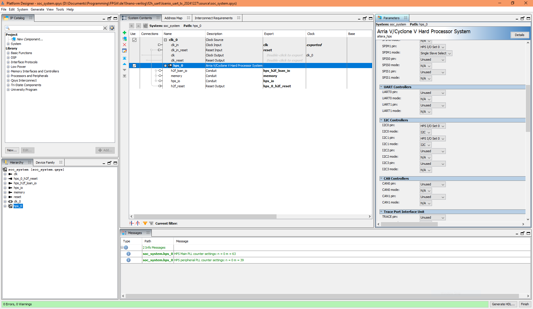
- Click or double-click the hps_0 to bring up the parameters panel
- Select "Peripherals Pins" tab, scroll down and change UART0 pin to "Unused". This disconnects the HPS UART0 I/O pins (wired to FT232R) from the HPS UART0 controller so that we can loan them out to the FPGA
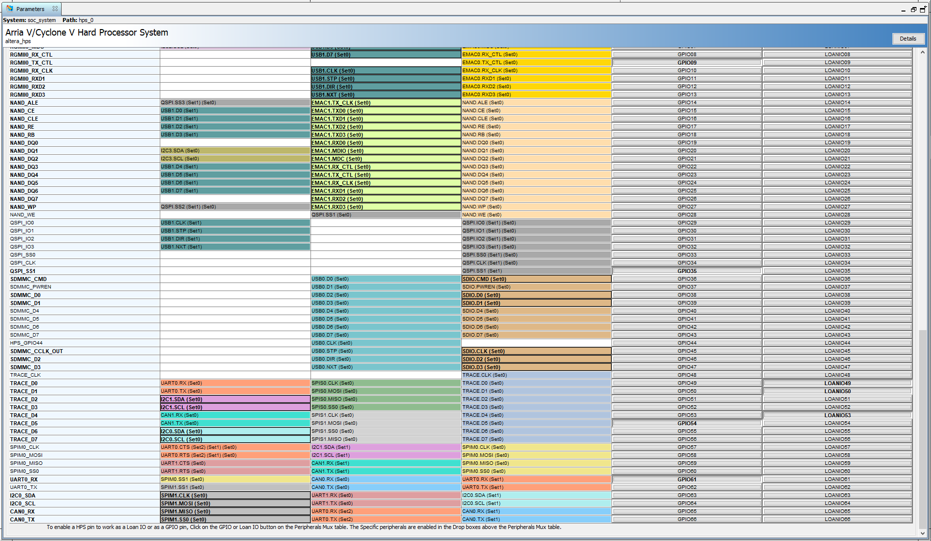
- Scroll to the bottom to see the "Peripherals Mux Table
- The last 2 columns lists 67 rows of buttons for selecting as GPIO or LOANIO
- Click on LOANIO49, LOANIO50 and LOANIO53
- Click on GPIO53 to deselect it
- Click "Finish" and "Yes" to generate now, or click "Generate HDL" and then "Finish". This generates and combines them into a single IP (IP variation named soc_system)
- Back in Quartus Prime, click "OK" to the prompt regarding the need to add .qip and .sip files
The .qip and .sip references are already in the existing project so there is nothing to do for that. In the "Project Navigator" panel select "Files" from the dropdown box, then you'll see the IP variation file soc_system/synthesis/soc_system.qip is already there.
UART0 pin set to Unused:
Peripheral Mux Table with loan I/O setting:
Logic for Serial UART
In the next step we need to modify the existing code or create new code. I have already created two separate example projects, one that can only transmit and another that can receive and transmit. It is easier if you just download and use my completed projects loanio_uart.
We need serial UART logic for the loaned I/O UART pins, instead of writing my own I have decided to use these nice lightweight serial modules by Dan Gisselquist. They needed a minor localparam modification for Quartus Prime to compile/synthesise:
Explanation of the code
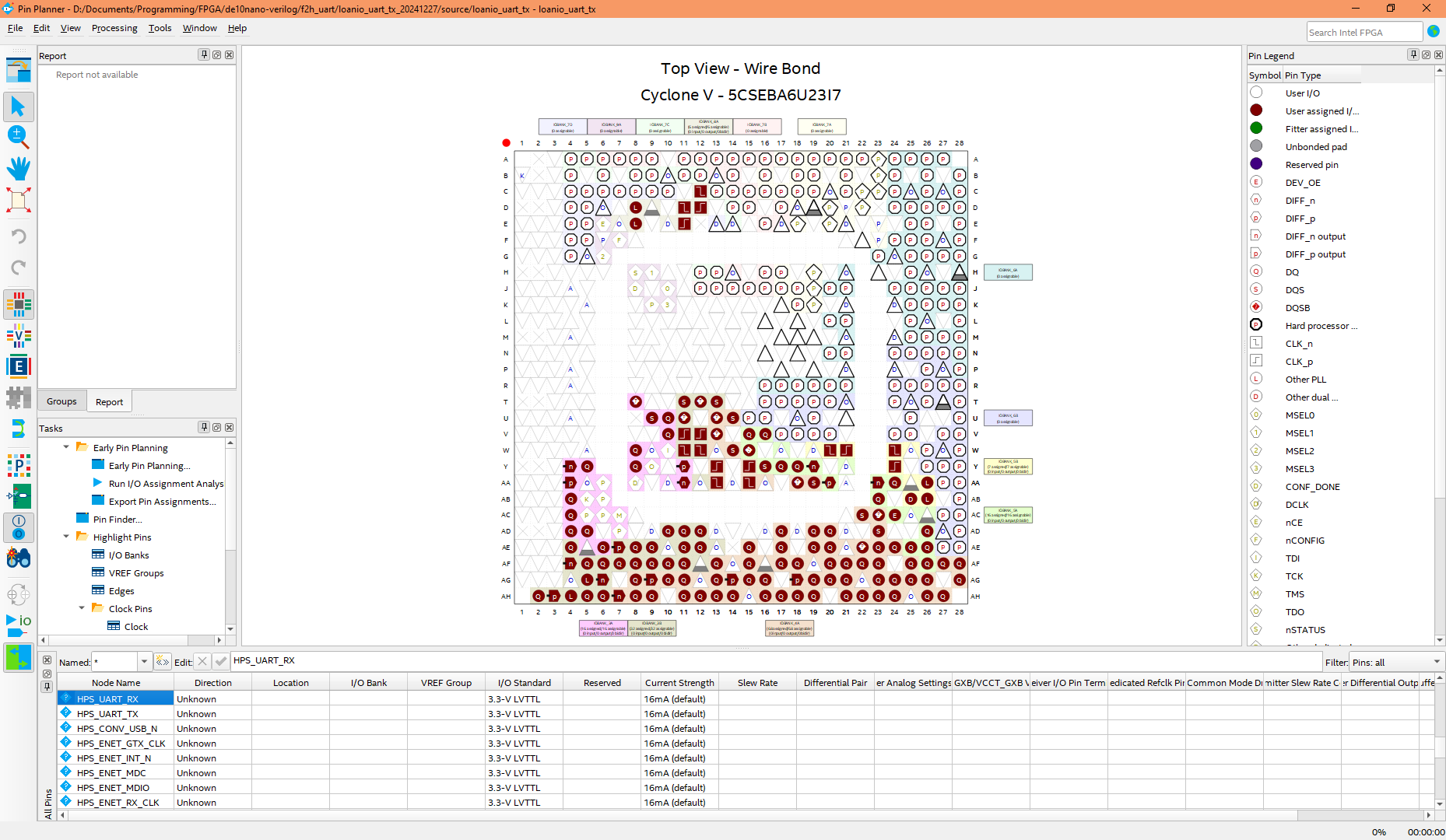
Most, if not all of the HPS pins require a configuration with no location and 3.3V LVTTL voltage level. They are set no location so that the compile process will use the hardcoded corresponding HPS pin - see the "Peripheral Pun Mux Table" for the mappings. All DE10-Nano HPS pins are already setup in the existing project, but from scratch you would create them using the "Pin Planner" or add manually in the .qsf file.
Pin Planner:
HPS GPIO and loan I/O pins require bidirectional mode wires, i.e. inout so at the top I modified the existing code with these:
                            inout HPS_UART_RX,

                            inout HPS_UART_TX,
Now we must becareful, the compile process will no longer prevent us from using the HPS_UART_RX as output, which can create a short if we output a voltage on it, because it is connected to the transmit pin of the FT232R.
After configuring the loan I/O, Platform Designer exports three port arrays for it, therefore these wires are added to our source to connect with them:
                            // Loan I/O IP ports

                            wire [66:0] loanio_oe;   // Pin direction: 0 = input, 1 = output

                            wire [66:0] loanio_in;   // Read port from pins: 1 = high, 0 = low

                            wire [66:0] loanio_out;  // Write port to pins: 1 = high, 0 = low
There are 67 elements in each array, one bit for each loan I/O pin, bit 0 for LOANIO0, bit 1 for LOANIO1, and so on. Only the loaned I/O pins configured in Platform Designer will be effective, so unconfigured bits do nothing.
Set direction mode of loan I/O pins
The loaned_oe array sets the pin direction, where 0 = input mode and 1 = output mode.
Read input from loan I/O pins
When the pin direction is set to input mode, for example assign loan_oe[49] = 0, then you can read input from the HPS pin using loanio_in[49], where 0 = low and 1 = high.
Write output to loan I/O pins
When the pin direction is set to output mode, for example assign loan_oe[50] = 1, then you can write output to the HPS pin using loanio_out[50], where 0 = low and 1 = high.
We need to wire loan I/O with the soc_system IP:
                            // HPS loan I/O IP ports

                            .hps_h2f_loan_io_in(loanio_in),

                            .hps_h2f_loan_io_out(loanio_out),

                            .hps_h2f_loan_io_oe(loanio_oe),


                            // HPS loan I/O pin connections

                            .hps_io_hps_io_gpio_inst_LOANIO49(HPS_UART_RX),

                            .hps_io_hps_io_gpio_inst_LOANIO50(HPS_UART_TX),

                            .hps_io_hps_io_gpio_inst_LOANIO53(HPS_LED),
We can now use the loan I/O pins just as you would with FPGA pins:
                            // ========================================================================================================

                            // UART transmitter and receiver (by Dan Gisselquist, see https://zipcpu.com/formal/2019/02/21/txuart.html)

                            // ========================================================================================================


                            reg       uart_tx_wr;

                            reg [7:0] uart_tx_data;

                            wire      uart_tx;

                            wire      uart_tx_busy;

                            txuartlite #(

                                .CLOCKS_PER_BAUD(434)  // = clk / baud = 50000000 / 115200

                            )

                            txuartlite_0(

                                .i_clk(FPGA_CLK1_50),

                                .i_reset(!master_reset_n),

                                .i_wr(uart_tx_wr),

                                .i_data(uart_tx_data),

                                .o_uart_tx(uart_tx),

                                .o_busy(uart_tx_busy)

                            );


                            wire       uart_rx_wr;

                            wire [7:0] uart_rx_data;

                            wire      uart_rx;

                            rxuartlite #(

                                .CLOCKS_PER_BAUD(434)  // = clk / baud = 50000000 / 115200

                            )

                            rxuartlite_0(

                                .i_clk(FPGA_CLK1_50),

                                .i_reset(!master_reset_n),

                                .i_uart_rx(uart_rx),

                                .o_wr(uart_rx_wr),

                                .o_data(uart_rx_data)

                            );


                            // ===================

                            // Configure loan I/Os

                            // ===================


                            // Set pin directions

                            assign loanio_oe[48:0]  = 0;  // Unused pins as inputs

                            assign loanio_oe[49]    = 0;  // UART_RX pin as input (LoanIO 49) *WARNING: do not set this to 1

                            assign loanio_oe[50]    = 1;  // UART_TX pin as output (LoanIO 50)

                            assign loanio_oe[52:51] = 0;  // Unused pins as inputs

                            assign loanio_oe[53]    = 1;  // HPS_LED pin as output (LoanIO 53)

                            assign loanio_oe[66:54] = 0;  // Unused pins as inputs


                            // Set I/O pin values

                            assign uart_rx = loanio_out[49];         // Read from pin

                            assign loanio_out[50] = uart_tx;         // Write to pin

                            assign loanio_out[53] = debounced_key0;  // Write to pin
Wiring loanio pin to serial receiver instance (serial input)
As you can see in the code, the loanio_in[49] is assigned to uart_rx wire so that serial data from the FT232R TX pin feeds the rxuartlite instance.
Wiring serial transmitter instance to loanio pin (serial output)
Similarly, the uart_tx wire is assigned to loanio_out[50] so that serial output from txuartlite feeds the FT232R RX pin.
Wiring key to loanio LED
The debounced_key0 is assigned to loanio_out[53] so key0 state outputs to the HPS_LED
Loan I/O not working?
This catches out many developers; by default loan I/O will not work if you run only the FPGA bitstream. The technical reference says loan I/O is held in a reset state and requires a preloader (configured via handoff settings) to make it available.
In older Altera software, the preloader configuration and compile process was automated using the SoC FPGA Embedded Development Suite (SoC EDS) and the BSP editor. These tools produced a compiled preloader, which is actually U-Boot image file (u-boot-with-spl.sfp) and was used for building the SD card image.
Those tools have been discontinued and replaced with a manual process: Building Bootloader for Cyclone V and Arria 10
Anyway, I've created my own automated SD card image process with some commandline scripts and make files. They are supplied together with my project files.
Debugging and U-Boot SPL
In the embedded world, U-Boot is a very large preloader good for putting onto an SD card, but not for loading with a debugger (e.g. JTAG + OpenOCD). Using OpenOCD, the USB-Blaster II JTAG is extremely slow and takes a very long time (several minutes) to load U-Boot!
U-Boot actually consists of two separate preloaders. It starts off with U-Boot SPL (a small preloader) which is designed to load into small embedded RAM to configure the basics, then it loads U-Boot (the big preloader) which takes over to configure everything else. Just for your knowledge, since U-Boot is isolated from U-Boot SPL it may reconfigure settings that were already configured.
A solution for OpenOCD is to use U-Boot SPL to configure the HPS and do away with the big U-Boot preloader counterpart. To do this we need to add CONFIG_OF_EMBED=y to the socfpga_de10_nano_defconfig, a configuration file found inside the U-Boot source files.
I've already included a prebuilt u-boot-spl, stored inside the bsp folder of my projects, but if want to build it yourself try the automated process with my ocram_ubootspl-build-make-scripts: DE10-Nano scripts. Ensure to update the HPS handoff folder (hps_isw_handoff) with the latest from your Quartus project.
HPS handoff files
When building the preloader, you will need to ensure to use the latest HPS handoff folder (hps_isw_handoff). I have found a possible bug, when changes are made in Platform Designer the handoff folder does not update (pin mux files not updated!), and is only updated when you compile the design in Quartus Prime.
Document date: Rev 1: 28 Dec 2024
