DE10-Nano: FPGA to HPS data transfer
Introduction
To explore the DE10-Nano development board further I decided on a new project. I would like to create one that streams data from the FPGA to the HPS.
These are my requirements defining the main functions of the project:
- Transfer data from FPGA embedded RAM to HPS SDRAM
- Transfer using the FPGA-to-HPS bridge (F2H bridge)
- Transfer using the FPGA-to-SDRAM interface (F2S interface)
- Find the fastest transfer throughput
- For data transfer complete, use an interrupt triggered from the FPGA
- Support sending parameters from the HPS to the FPGA
- Use a hardware timer to measure transfer throughput
- Verify the transferred data
Gathering information
Documents with useful information
Since I am a total beginner of FPGA + SOC I did have a hard time with new stuff, but it was fun perusing through all those technical manuals and projects examples. Here is a review of my findings.
Interconnecting data bus
On the Cyclone V SoC FPGA there are four types of data buses where data can cross the two fabric:
| Data bus | Number of ports | Master data width (in bits) | Slave data width (in bits) | Protocol |
|---|---|---|---|---|
| FPGA-to-HPS bridge (F2H bridge) | 1 | 32, 64, or 128 | 64 | AXI-3 |
| FPGA-to-SDRAM interface (F2S interface) | 1 to 3 (AXI-3) or 1 to 6 (Avalon-MM) |
32, 64, 128, or 256 (total limited to 256) | 64, 2x64, or 4x64 | AXI-3 or Avalon-MM |
| HPS-to-FPGA bridge (H2F bridge) | 1 | 32, 64, or 128 | 64 | AXI-3 |
| Lightweight HPS-to-FPGA bridge (L2F bridge) | 1 | 32 | 32 | AXI-3 |
Since we want to transfer from the FPGA to the HPS we can use either the F2H bridge or the F2S interface to write data into the HPS SDRAM. The F2S offers two protocols, but I will use the AXI-3 protocol because it is available for all data buses.
Cache maintenance
When L1 or L2 data cache are enabled data transfers between the FPGA and the HPS SDRAM must be managed, whether manually or automanaged depending on the bridge (data bus) and memory map.
Data transfer over the F2H bridge and ACP memory map
SDRAM access through the F2H bridge is cache coherent but only when used with the ACP memory map. With this method we don't need to apply any cache maintenance ourself.
The ACP memory map is provided by the ACP ID Mapper (A HPS component) which provides and manages a 1GB cache coherency window, and it also maps 12-bit AXI IDs for this to work.
The ACP ID Mapper is connected to the CPU core through the Accelerator Coherency Port (ACP) (An ARM MPCore component) that is integrated inside the Snoop Control Unit (SCU). On the FPGA side, read & write access requests are made with the F2H bridge, passed to the ACP ID Mapper to generate corresponding AXI requests, sent into the ACP, which then works with the SCU to make the actual cache coherent access with the SDRAM.
The 1 GB cache coherent window (SDRAM memory map) that is facing the ACP is remappable within the 4 GB Arm Cortex-A9 MPCore address space. By default it is mapped to the bottom of the SDRAM, i.e. address range: 0x00000000 to 0x3FFFFFFF.
The 1 GB cache coherent window (ACP memory map) that is facing the F2H bridge however is fixed, and is located at the 1 GB address range: 0x80000000 to 0xBFFFFFFF. To use the 1 GB cache coherent window we simply write into the fixed ACP memory map range using the F2H bridge with correct AXI-3 AxUSER and AxCACHE settings. For the details see "Accelerator Coherency Port" in the "Cyclone V Hard Processor System Technical Reference Manual" and the "Arm Cortex-A9 MPCore Technical Reference Manual".
Data transfer over the F2S interface
In comparison, the F2S interface provides a much wider data bus than the F2H bridge, but the requests are made directly to the SDRAM controller and so there is no builtin cache coherency support. The HPS must do one of the following in order to see updated data transfers in SDRAM:
- issue L1/L2 data cache flush/clean before a data transfer or
- set an area of SDRAM to be noncacheable via the Memory Management Unit (MMU) or
- disable L1/L2 data cache
FPGA embedded memory
FPGA data acquisition normally require memory buffer capable of working at the acquisition clock frequency. The DE10-Nano does not have RAM connected to the FPGA side, but the FPGA itself has some embedded memory (internal memory).
The Cyclone V SoC FPGA model 5CSEBA6U23I7 has 553 blocks of M10K embedded memory bits, which gives total memory of: 553 * 10K = 553 * 10240 = 5662720 bits = 707840 bytes. I will be using slightly less than that because we need to align with the largest transfer size.
I will use the AXI-3 protocol to transfer data to the HPS. It is capable of performing 1-16 bursts of write transactions. We will get the highest throughput if we use the largest burst length of 16 together with the largest data bus width. This table shows the largest transfer sizes of each data bus:
| Data bus | Transfer size per burst | Transfer size of 16 bursts |
|---|---|---|
| F2H bridge | 128 bits = 16 bytes | 16 * 128 bits = 2048 bits = 256 bytes |
| F2S interface | 256 bits = 32 bytes | 16 * 256 bits = 4096 bits = 512 bytes |
| H2F bridge | 128 bits = 16 bytes | 16 * 128 bits = 2048 bits = 256 bytes |
| L2F bridge | 32 bits = 4 bytes | 16 * 32 bits = 512 bits = 16 bytes |
Using the FPGA embedded memory
FPGA embedded memory can be utilised using a suitable Intel IP, available within the Platform Designer under "Basic Functions/On Chip Memory".
Alternatively, embedded memory can be utilised directly within your own Verilog logic code using either a special synthesis attribute or a synthesis comment. For details see Quartus® Prime Pro Edition Help: ramstyle Verilog HDL Synthesis Attribute. My m10k_mem.v Verilog module implements it this way.
The attribute tells the Analysis & Synthesis to implement the register array (inferred as RAM) using embedded memory instead of logic. Note it may fail to implement using embedded memory when restrictions are not met, such as the read and write must be clocked, the register must be an array, the register must be not be larger than the available embedded memory.
Vendor IP limitations
Typically to save time we would use the vendor's IP (Intel IP) over implementing our own Verilog logic. For data transfers these Intel IP categories can be used:
- "Basic Functions/On Chip Memory"
- "Basic Functions/DMA"
- "Processors and Peripherals/Peripherals/PIO (Parallel I/O) Intel FPGA IP"
Since I want to obtain maximum throughput I would like to use 2048 and 4096-bit data widths, unfortunately none of the "On Chip Memory" Intel IPs support such large sizes. I will need to write my own Verilog logic for it.
There is a very nice project created by Roberto Fernández Molanes many years ago, who has designed the hardware mainly with the Intel IPs in Platform Designer CycloneVSoC-time-measurements. It will be interesting to compare the results.
Project design
To test the two data buses, it was easier to implement separate projects, one for the F2H bridge and another for the F2S interface.
FPGA hardware design
The design is implemented using Verilog and minimum Intel IPs. There is a main top.v file with the main control logic and the rest are separate module files.
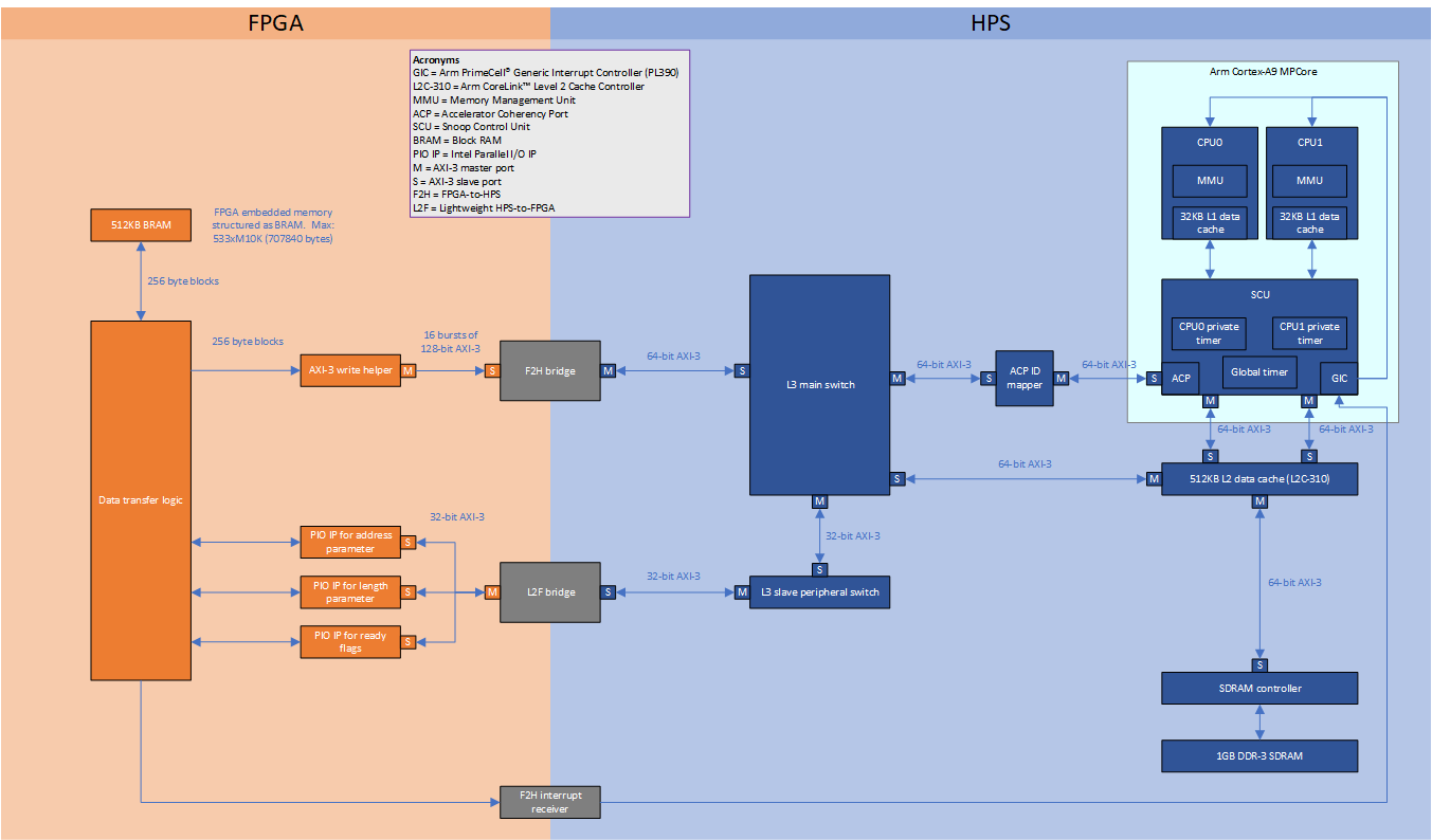
This block diagram shows the flow and connections between the logic from the FPGA to the HPS for the F2H bridge + ACP design:
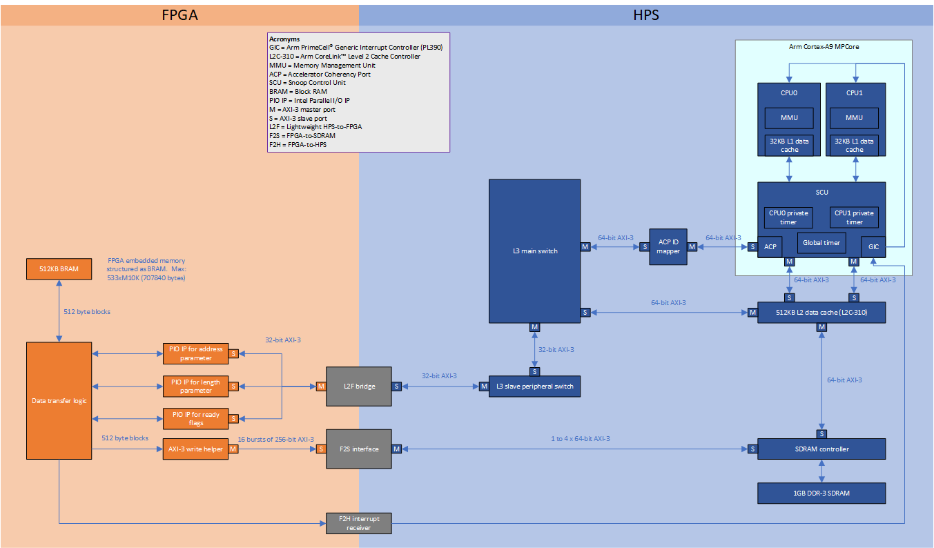
This block diagram shows the flow and connections between the logic from the FPGA to the HPS for the F2S interface design:
Some components ommitted for simplification.
In the FPGA (orange coloured side) we have the following component logic:
BRAM
Represents my custom Verilog module implementing a block RAM with FPGA embedded memory. This memory buffer will store and buffer the test data to be transferred to the HPS SDRAM. The block RAM is organised linearly with fixed size blocks starting from address 0.
The block size (data width) is configured to align with 16 bursts of write AXI-3 transactions with the largest data bus width as follows (respectively for each project):
- 128-bit F2H bridge: 128-bit * 16 bursts = 2048 bits = 256 bytes
- 256-bit F2S bridge: 256-bit * 16 bursts = 4096 bits = 512 bytes
Parallel IO IP (PIO IP) & L2F bridge (passing parameters)
The Intel PIO IP provides an easy way to use the L2F bridge for exchanging low bandwidth data. My FPGA design will wait for the length parameter to be non-zero and the ready flag to signal before it will actually start transferring. This IP provides memory mapped registers for the HPS to send parameters to the FPGA without us needing to work with the AXI-3 (L2F bridge) directly.
Parallel IO IP (PIO IP) & L2F bridge (passing ready flags)
For synchronization between the FPGA and HPS I use ready flags as signals. The flags enable the HPS to signal the FPGA when the next transfer can start and when to de-assert the interrupt trigger.
AXI-3 write helper
This is my custom Verilog module which implements a simple AXI-3 master write only controller. It will write data from a register over AXI-3. It is used here for transferring blocks of data from the BRAM to the HPS over the F2H bridge or F2S interface. Essentially a primitive IP that achieves the same result as an Intel DMA IP.
HPS software design
The software on the HPS has a master role and the hardware design on the FPGA has a slave role. The FPGA waits for a signal before starting the transfer process. The HPS controls the transfers, when a transfer completes the FPGA triggers an interrupt, and the HPS handler executes, which measures the throughput, reads and verifies the data in the SDRAM buffer. It is interrupt and preemptive task (FreeRTOS) driven.
Parameter transfer
Parameters and flags are transmitted between the two sides over the Lightweight HPS-to-FPGA bridge (L2F bridge), accessed with the Parallel IO IP (PIO IP), which provides memory-mapped registers for the HPS.
Ready flag and synchronization
Two separate ready flags are used for acknowledgement between the two sides. They are organised as a 2 position cyclic buffer, where after a complete data transfer, each side (FPGA and HPS) switches to an opposite index. This ensures that each side always use a different ready flag which prevents the synchronisation problem of a flag being read and written at the same time.
F2S interface cache coherency
Since the F2S interface does not support cache coherency access, I have decided to set the SDRAM buffer region to non-cacheable using MMU table entries.
The process flow
- The compiled hardware design file is downloaded to the FPGA
- The HPS application is executed
- The FPGA fills the BRAM (M10K embedded memory) with test data
- The FPGA is now in a waiting state; waiting for the HPS to send parameters and the ready signal before it starts transferring
- The HPS application send parameters to the FPGA, starts a preemptive control task, starts a timer and asserts the ready signal
- The FPGA transfers data from FPGA BRAM to HPS SDRAM buffer defined by start address and size parameters received from HPS earlier
- When the transfer size is reached the FPGA asserts an interrupt trigger to generate one on the HPS, and then enters into a waiting state
- The IRQ is raised on the HPS which jumps into the interrupt handler. The handler stops the timer, deasserts the ready signal to indicate the FPGA to deassert the interrupt trigger, and then signals the preemptive control task to process the data
- The FPGA switches to another ready flag
- The control task calculates the throughput of the transfer and verifies the transferred data
- If the test is not yet complete, the task switches to another ready flag, and asserts the ready signal for the FPGA to start another transfer, repeating the process
Some technical details:
- FreeRTOS provides the preemptive control task and synchronization
- The FPGA triggers HPS GIC IRQ 72 interrupt (aka FPGA IRQ 0 on the FPGA side)
- Arm MPCore Global Timer for measuring the data transfer. Alternatively, we can use one of the four HPS peripheral timer, but in comparison those are 32-bit counter timers vs the Arm MPCore a 64-bit counter timer.
Project files
My project is located here: fpga_to_hps.
Results
The results are surprising, I get extremely fast throughput! Note, the F2H & F2S data bus runs perfectly fine at 200MHz and there is no data corruption, verified by running an incremental counter check. If this wasn't a hobby I would run a more thorough check using a LFSR based random generator + random seed instead.
F2H bridge + ACP results
Test configuration:
FPGA: 128-bit F2H bridge at 200MHz
HPS: L1+L2 caching enabled in the software
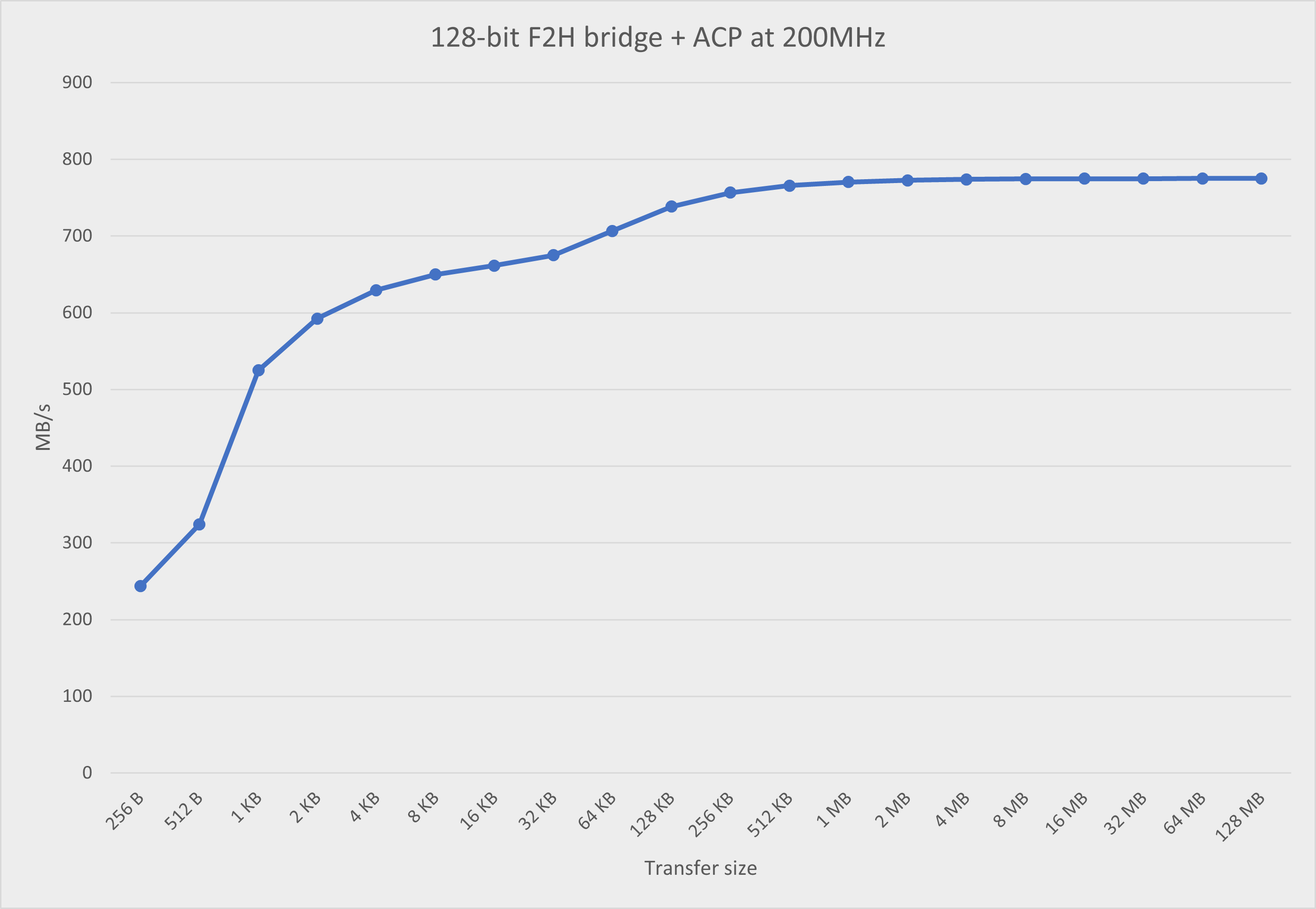
The results are put into this chart.
Let's compare with the CycloneVSoC-time-measurements project. We can compare with the read transfer results from his Excel file.
The highest throughput rate from my project:
F2H bridge, 128-bit, 200MHz, 64KB: 706.50 MB/s
F2H bridge, 128-bit, 200MHz, 128MB: 775.01 MB/s
The highest throughput rate from the CycloneVSoC-time-measurements project:
F2H bridge, 128-bit, 50MHz, 64KB: 54.21 MB/s
F2H bridge, 128-bit, 100MHz, 64KB: 71.53 MB/s
F2H bridge, 128-bit, 150MHz, 64KB: 81.79 MB/s
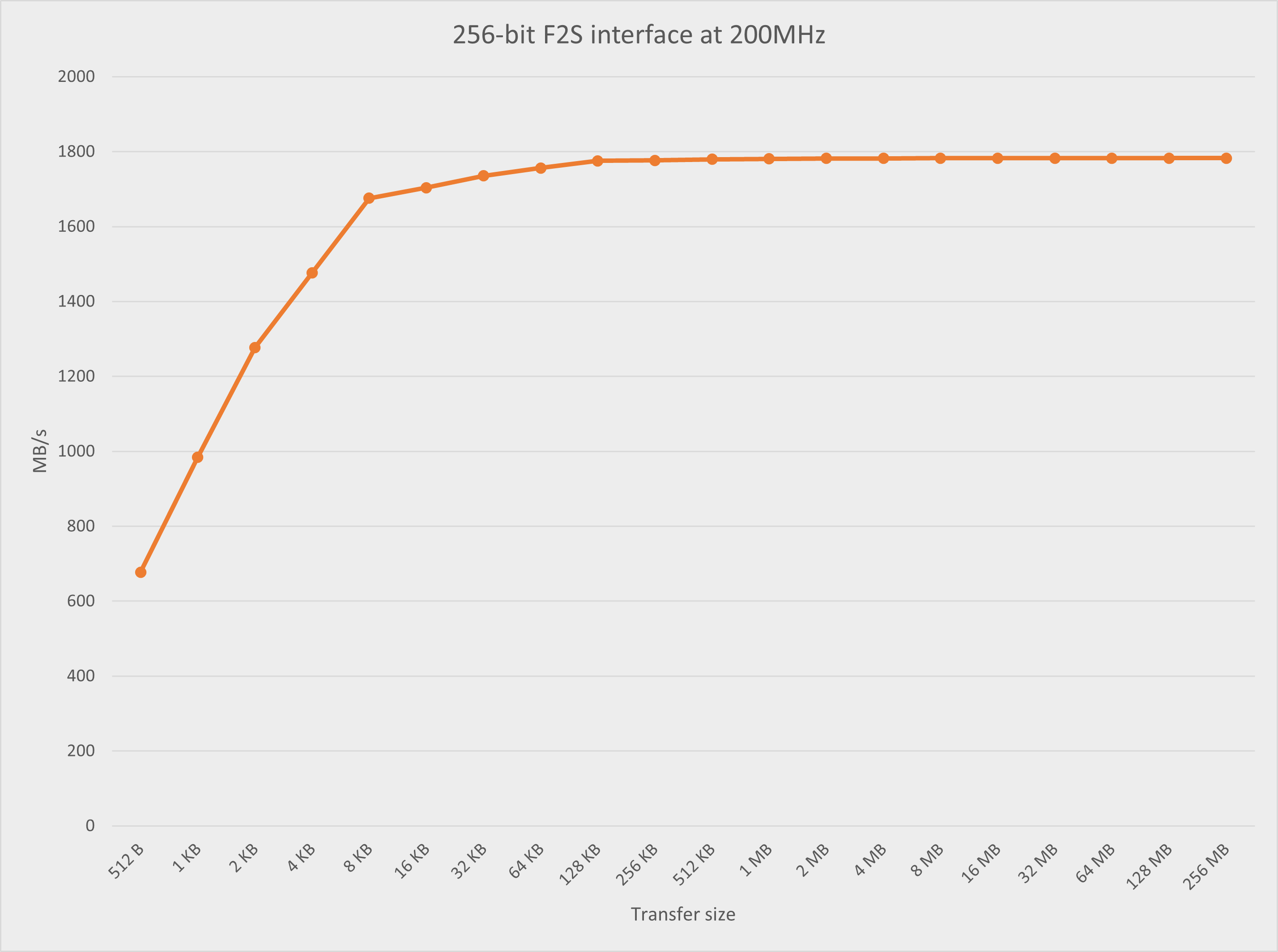
F2S interface results
Test configuration:
FPGA: 256-bit F2S interface at 200MHz
HPS: L1+L2 caching enabled in the software and the buffer region set to non-cacheable
The results are put into this chart.
The highest throughput rate from my project:
F2S interface, 256-bit, 200MHz, 2MB: 1781.89 MB/s
F2S interface, 256-bit, 200MHz, 256MB: 1782.62 MB/s
The highest throughput rate from the CycloneVSoC-time-measurements project:
2x F2S interface, 2x128-bit, 50MHz, 2MB: 597.22 MB/s
2x F2S interface, 2x128-bit, 100MHz, 2MB: 984.28 MB/s
2x F2S interface, 2x128-bit, 150MHz, 2MB: 1452.90 MB/s
- Terasic DE10-Nano kit board information
- FreeRTOS Kernel API Reference
- Intel SoC FPGA HWLIB
- Intel Embedded Peripherals IP User Guide, PIO Core
- Intel Cyclone V Hard Processor System Technical Reference Manual
- Arm PrimeCell Generic Interrupt Controller (PL390) Technical Reference Manual
- Arm Cortex-A9 MPCore Technical Reference Manual
- ARM Architecture Reference Manual ARMv7-A and ARMv7-R edition (Cache and MMU registers)
- Quartus® Prime Pro Edition Help: ramstyle Verilog HDL Synthesis Attribute
Document date: Rev 1: 15 Oct 2024
