Using the HPS (processor) UART peripheral directly from the FPGA side on the Terasic DE10-Nano development kit
Introduction
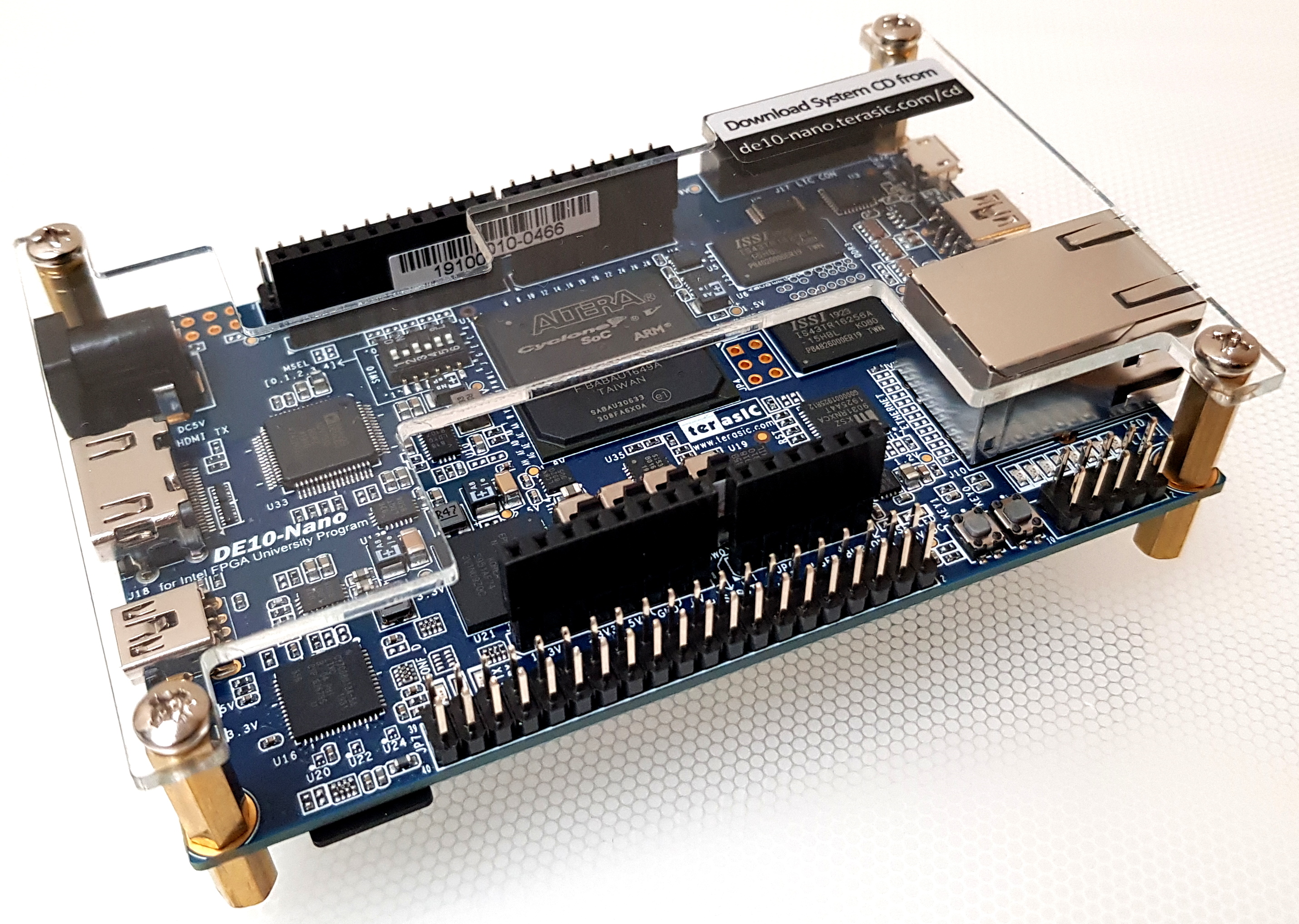
Last year in 2020, I received a DE10-Nano development kit (an electronic test development board) from a friend, who sent it all the way from the Netherland to the UK. Thanks to him I got to play with this rather interesting FPGA kit.
I have tinkered with FPGA in the past, but to my surprise this is a different beast. The kit contains an Altera (now acquired by Intel) Cyclone V series FPGA with integrated SoC (System on Chip) all inside a single chip.
It seems acronyms and new words is the trend these days, but we will have to use them to keep up with the literature out there. The acronym SoC here refers to an ARM processor system which consists of a Dual ARM processor (800MHz Cortex-A9 in this case), the interconnection buses, DMA controller, interrupt controller, peripherals such as USB, SDRAM, Ethernet, etc. So this is not a plain FPGA, it is a combo (a 2-in-1) FPGA with an integrated ARM processor system. Altera calls this architecture SoC FPGA, and the SoC part is called the HPS (Hard Processor System). See below a block diagram showing the distinct FPGA and HPS areas.
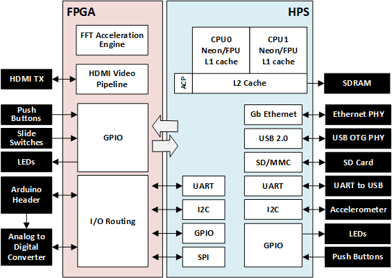
After implementing some projects with this kit, I quickly discovered that many of the peripherals are connected only to the HPS side. These are all of the peripherals inside the blue coloured side of the block diagram, for instance the UART-USB, USB-OTG, and Ethernet controllers. They are accessed through software running on the processor (HPS side), and not directly accessible on the FPGA side. When running a Linux system on the kit, the peripherals are accessed through supplied linux drivers, if developing plain application, i.e. without an OS (aka bare-metal) then most peripherals can be accessed with Altera's HWLibs (C library). Both methods are really accessing the peripherals through memory mapped registers from hard-IP (hardware) controllers called HPS peripheral controllers, and these are baked-in (fabricated) into the SoC IC. These controllers were originally created from software FPGA IP designs and then turned into hardware called hard-IP - many of them are FPGA IP designs from Synopsys, specifically, part of their DesignWare IP product. There is very little or no technical information publicly available.
In every Quartus Prime project the HPS is modelled as an IP module that you have to instantiate (i.e. create) in Quartus Prime Platform Designer, and is also where the settings can be configured. The HPS instance is configured by a right-click edit or a double-click, which displays the parameters dialog or tab. There is also a "Peripheral Pins" tab with options to configure the routing of the HPS peripheral controller IP pins in various ways:
| Parameter | Routing | Description |
|---|---|---|
| HPS IO set | HPS peripheral controller IP to use a pin located on the HPS side (HPS I/O pin). Each group of HPS I/O pin is identified by a HPS I/O set number. | Configures the HPS peripheral controller (hard IP) to use the dedicated HPS I/O pins making it standalone. The HPS can use its peripheral controller without requiring the FPGA. The FPGA side does not have access these pins. |
| FPGA | HPS peripheral controller IP to use a logic ports on the FPGA side. This is basically HPS peripheral controller IP port pins exported to the FPGA side. | Configures the HPS peripheral controller (hard IP) to use pins defined by FPGA logic. The HPS should not use the controller until the exported ports are configured by the FPGA - that is because the FPGA must apply logic to them, e.g. assign them to FPGA hardware pins or just logic. Comparing to the HPS I/O set option, the HPS peripheral controller can use FPGA pins (alternate pins to the predefined ones). Note the port pins remain accessible by the FPGA. A use case for this is the FPGA can intercept, log, modify or dynamically route (multiplex) the HPS peripheral controller port pin, doing this transparently while the HPS is using the controller. |
| GPIO | HPS GPIO peripheral controller IP to use a HPS I/O pin. Any of the unused 67 HPS pins can be selected for HPS GPIO via buttons within the Peripheral Mux Table. | Configures the dedicated HPS I/O pins to be mapped to memory addresses, which enables the HPS with its GPIO peripheral controller (hard IP) to control them as general I/O. |
| Loan IO | HPS I/O pin as exported ports on the FPGA side. Any of the unused 67 HPS pins can be selected for Loan I/O via buttons within the Peripheral Mux Table. | Configures the dedicated HPS I/O pins to be routed to FPGA port I/O array, which enables the FPGA to control them as general I/O. |
In the DE10-Nano's schematics we see that many of the peripherals on the PCB such as UART-USB, USB, and Ethernet are physically wired to predefined HPS pins (HPS I/O set), and if we wish to directly use the HPS attached peripheral pins from the FPGA side we can use the loan I/O. In the previous versions of this document I was wrong about the loan I/O not usable to control the HPS peripheral. I confirm it is possible and will make a guide for that soon. *Update: available here use loanIO + UART verilog HDL with the existing HPS peripheral directly
There is another a way to use the peripherals from the FPGA side, and that is by driving the registers of the HPS peripheral controller through the FPGA-to-HPS bridge, since the bridge and peripherals are in a reset state on startup, this require the HPS to be initialised first, which I've utilised with U-Boot SPL. There are guides for using the HPS peripherals (HPS controller) on Linux system and a few for bare-metal example source codes, but none on FPGA. Cyclone V SoC FPGA was released a long time ago, I'm really surprised that no one has found a way to do this - perhaps my source is the first solution. I present you a demonstration Verilog Quartus Prime project where the FPGA is able to send a serial transmission (message) using the HPS UART controller!
Source files
Consists of a Quartus Prime v21.1 project containing the Verilog source files which can be downloaded from my github account.
Running instructions
Download the source file or browse the files on the github and you should find a prebuilt SD card image file inside the folder sdcard_image.
- Write the sdcard_de10nano.img to a micro SD card. Use any of these:
- Connect a USB-B micro cable between the UART-USB connector on the DE10-Nano and your computer
- Start a serial console program such as PuTTY and set it to serial mode and the correct COM port, 115200 baud, 8 data bits, 1 stop bit, no parity, no control flow
- Insert the micro SD card into the DE10-Nano and turn on the 5V power supply
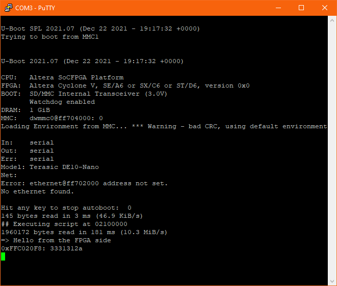
- Wait for U-Boot to boot up. You should see a bunch of U-Boot messages, runs a script to configure (program) the FPGA and enable FPGA and HPS bridges, then stops at a console prompt
- The FPGA logic side should be configured at this point and LED7 should be blinking now
- Press and release key0 on the DE10-Nano and you should see a hello message - this comes directly from the FPGA logic side!
Note, I've configured U-Boot to boot only to the console prompt - there is no Linux system.
Here's what you should see in PuTTY:
Source file guide - parameters
The HPS UART is accessed from the FPGA side through the FPGA-to-HPS bridge, which is basically a memory mapped bus connection and enables the FPGA to read and write the HPS memory address map. This bridge is accessed using ARM's AXI communication interface protocol. The AXI interface includes quite a handful of signals, to simplify things I created read and write AXI helper Verilog modules.
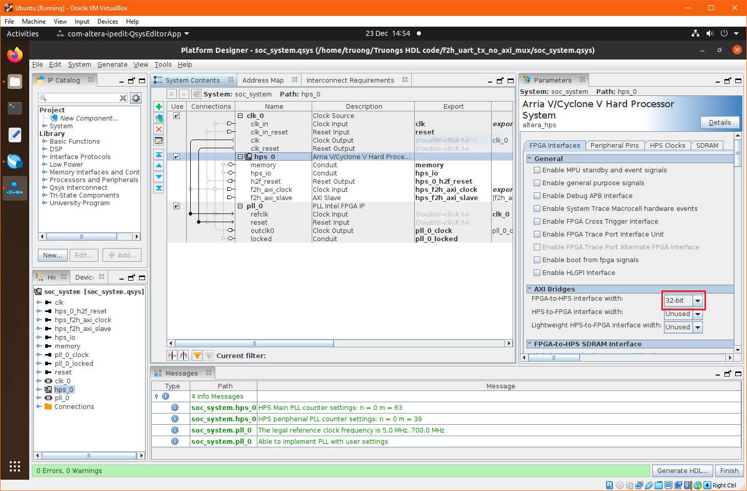
The rd_axi.v and wr_axi.v modules are fairly basic, but ensure that the parameters RD_AXI_BUS_WIDTH and WR_AXI_BUS_WIDTH are set to the same value as the FPGA-to-HPS interface width in Platform Designer.
The uart_dev.v is the interesting module, it takes care of the serial transmission. It accepts input in two ways: a register or a memory address, both are demonstrated in the top level file top.v. For the first option, the parameter UART_DATA_BUF_LEN determines the size of the input register to be synthesized. Note: string literals in Intel FPGA Quartus Verilog are stored with the left most character in the highest byte position. This code takes the input character string and transmits them in the reverse order, i.e. from lowest byte position first because I think this is more natural.
Input parameters of uart_dev.v:
| Parameter | Description |
|---|---|
| enable | 1 = transmit, 2 = receive, 0 = do nothing |
| tx_input_type | selects data source type: 0 = data buffer register, 1 = memory address offset |
| tx_data | register containing data to transmit. Selected when tx_input_type = 0 |
| tx_addr | address of memory containing data to transmit. Selected when tx_input_type = 1. Address must be 32-bit aligned, i.e. must be a multiple of 4 |
| tx_len | length of transmit data in bytes |
| tx_hex | converts bytes into hex string: 0 = no, 1 = yes |
| tx_hex_start | starting position to convert into hex string. First position is 0 |
| tx_new_line | transmit new line at the end: 0 = no, 1 = yes |
Output parameters of uart_dev.v:
| Parameter | Description |
|---|---|
| rx_data | register containing byte received |
| status | 0 = none, 1 = busy, 2 = done transmit or received data, 3 = done but no received data |
Source file guide - transmit steps
Since the HPS UART controller is designed for a processor the operations are sequential. A common approach to simulate a sequence of operations from the parallel nature of FPGA is to write a Finite State Machine (FSM). The basic steps to send a transmission using the uartdev.v module is as follows:
- set the input parameters
- wait for status to become 0 (indicates UART transmit buffer is ready)
- set enable = 1
- wait for status to become 2 (indicates transmission done)
- set enable = 0
- if more to send then repeat from step 1
I suggest a look at the top level file top.v to see how this is done.
This code snippet is what transmits the hello message (a section of the FSM):
                localparam UART_HELLO_MSG_LEN = 26;
                localparam [8*UART_HELLO_MSG_LEN-1:0] uart_hello_msg = "Hello from the FPGA side\r\n";
                ...
                case(state)
                    ...
                    1: begin
                        ...
                        uart_msg_counter <= UART_HELLO_MSG_LEN - 1;
                        ...
                    end
                    ...
                    // STATE: transmit string message to UART
                    2: begin
                        case(uart_status)
                            0: begin
                                uart_data <= uart_hello_msg[8*uart_msg_counter +: 8];
                                uart_input_type <= 0;
                                uart_data_len <= 1;
                                uart_hex <= 0;
                                uart_new_line <= 0;
                                uart_enable <= 1;
                            end
                            2: begin
                                uart_enable <= 0;
                                if(uart_msg_counter > 0) begin
                                    uart_msg_counter <= uart_msg_counter - 1;
                                end
                                else begin
                                    uart_msg_counter <= UART_ADDR_MSG_LEN - 1;
                                    state <= state + 1;
                                end
                            end
                        endcase
                    end
                ...
                endcase
Explanation: A hello message is stored in a register at the beginning. Case 1 initialises a counter to the length of the message less 1. Case 2 creates a loop based on the uart_status to send each character and stops when the counter reaches 0.
This code snippet transmits the content of 4 memory addresses starting from address 0xFFC020F8 (a section of the FSM):
                // STATE: transmit RAM content (4 bytes in hex format) to UART
                4: begin
                    case(uart_status)
                        0: begin
                            uart_input_type <= 1; // Read from FPGA-to-HPS bridge AXI address
                            uart_addr <= 32'hFFC020F8; // UART Controller Version
                            uart_data_len <= 4;
                            uart_hex <= 1; // Display as hex string
                            uart_new_line <= 1; // Display a new line
                            uart_enable <= 1;
                        end
                        2: begin
                            uart_enable <= 0;
                            state <= 0;
                        end
                    endcase
                end
Explanation: The uart_dev module takes care of character (or byte) looping in this case and a counter is not required here. Note uart_input_type is set to 1 and uart_data_len is set to 4. After enabling the transmission, we simply wait for uart_status to become 2.
Limitations and to do list
This initial version is very basic. I wanted to quickly get a proof of concept and so there are many limitations:
- Relies on SD-card + U-Boot to configure the serial port during its boot up
- Only implements serial transmission
- Polling method is used to determine whether the UART is ready
I hope to get around to doing this do list:
- Remove the need for SD-card + U-Boot by directly configuring the serial port from the FPGA side. *Update: this is not possible because AFAIK the FPGA-to-HPS bridge can only be enabled with code on the HPS side - a workaround is to boot from FPGA and have it run HPS code (e.g. U-Boot SPL) stored in OCRAM or EPCS
- Serial reception
- Replace the polling by using the controller's interrupt (UART interrupt in this case), which can be enabled (forwarded) to the FPGA side
HPS bridge max clock speed limitation
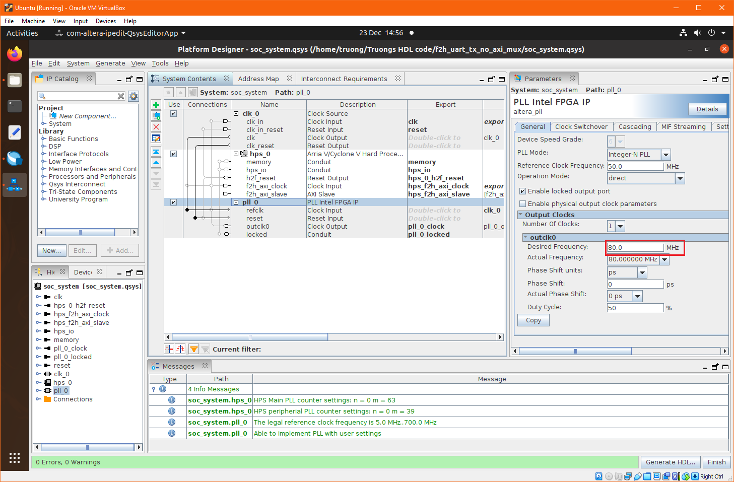
The FPGA-to-HPS bridge interface requires a user supplied clock (pll_0 in my case), but it seems the HPS peripheral controllers only work upto a particular maximum clock speed. I have observed strange behaviour and wasted a lot of debugging time (FPGA logic behaving incorrectly) when using the HPS USB & UART from the FPGA side with 150MHz and also sometimes with 100MHz clock. At 80MHz it seems to be stable.
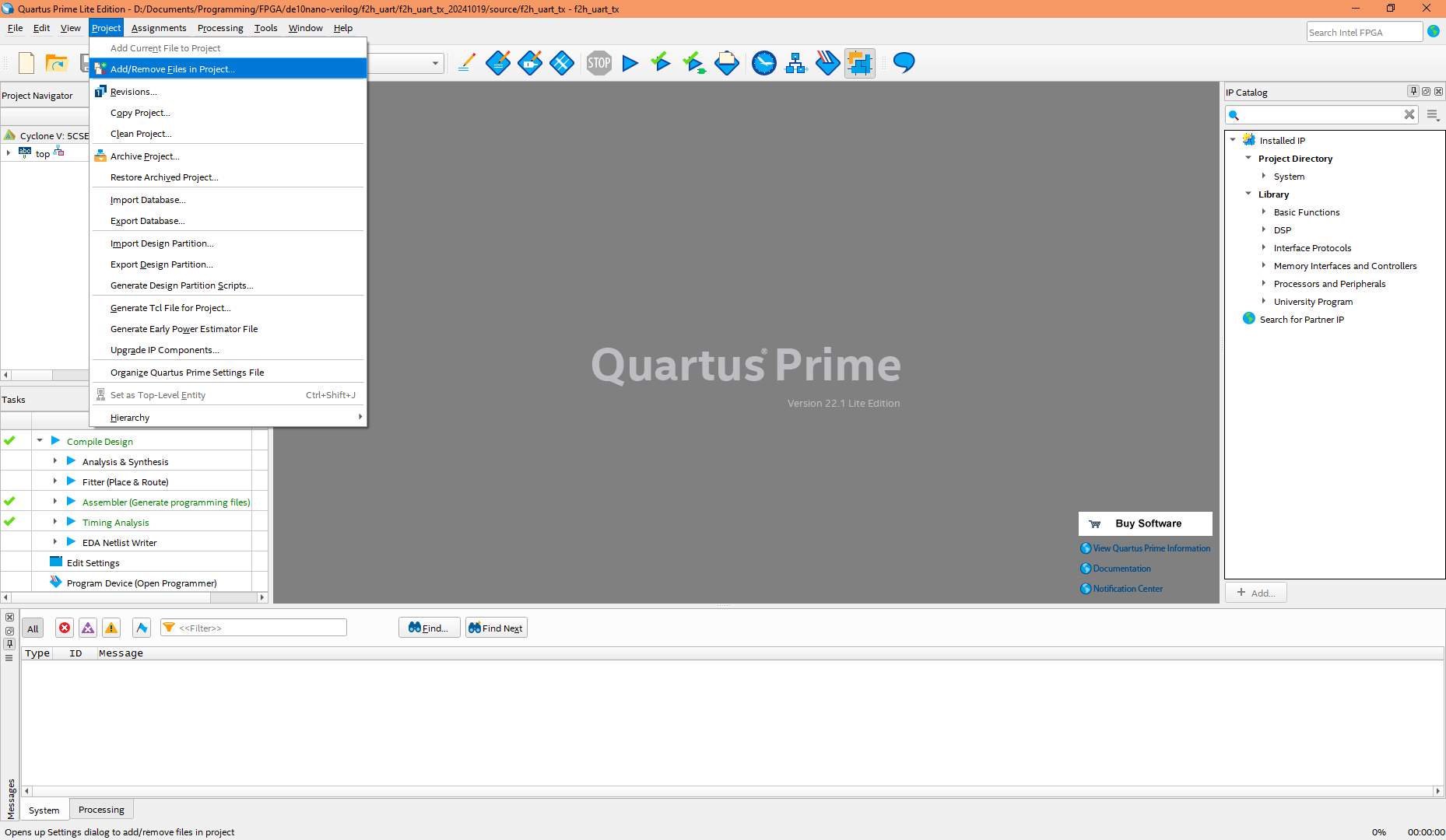
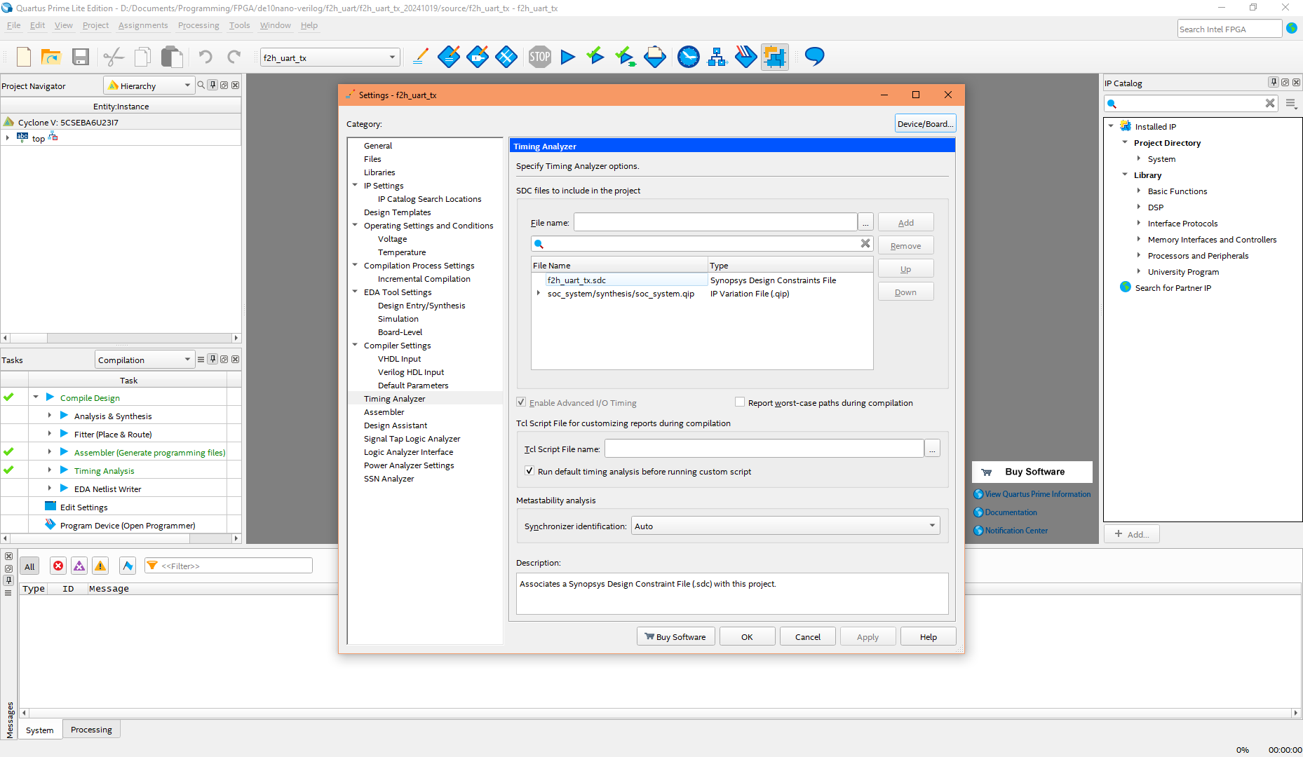
*Update (26/10/2024): I didn't realised we have to include a .sdc (Synopsys Design Constraint) file to the project manually which is required when using higher frequencies, else we get data corruption due to timing. After adding this file, I am able to use a maximum of 200MHz frequency working reliably for any of these interfaces:
- FPGA-to-HPS bridge
- HPS-to-FPGA bridge
- Lightweight HPS-to-FPGA bridge
- FPGA-to-SDRAM controller interface
Inspired future project
I am currently working on another project, this time, trying to get the FPGA side to directly use the HPS USB 2.0 OTG controller in device mode. This is a more difficult task and involves dealing with the USB protocol, descriptors and setup packets. It will enable the FPGA side to directly transfer data between the host computer at high speed.
Appendix
| Acronym | Description |
|---|---|
| SoC | A computer system implemented as a hardware circuit. It is designed to be integrated to another hardware such as FPGA. |
| FPGA | Field-Programmable Gate Array. A hardware circuit mainly of logical gates that a user can configure and thus is analogous to rewiring or configuring the circuit (reprogram if you like). Gate configuration is done by downloading a compiled hardware design FPGA configuration file. |
| HPS | Hard Processor System. In the system block diagram, HPS is the block portion representing the computer system (SoC). |
| HDL | Hardware Design Language. A human understandable language for describing and coding a hardware design, which can then be compiled (converted) to produce a FPGA configuration file. The most popular languages are VHDL, Verilog and System Verilog. |
| UART | Universal Asynchronous Receiver-Transmitter. The old standard serial communication protocol. |
| FSM | Finite State Machine. A group of conditional statements simulating a sequence of operations with a fixed number of possible states. It is usually implemented with case statements but can also be done with multiple if and else statements. |
| Module ports | The input and output parameters of a module, representing things such as registers, wires, or pins. |
Document date: Rev 4: 27 Dec 2024 - Loan I/O correction Document date: Rev 3: 03 Nov 2024 - Peripheral Pins description made simpler
Document date: Rev 2: 26 Oct 2024 - Constraint file and max frequency discovered
Document date: Rev 1: 23 Dec 2021
