DE10-Nano: Multiprocessing application (AMP system)
Introduction
The DE10-Nano board contains a dual core ARM Cortex-A9 processor, which we can utilise with multiprocessing capable programs. So far we have only been running uniprocessing programs on core 0 (CPU 0). It would be nice if we can execute a second program on core 1 (CPU 1).
The two well-known systems that makes use of multiple processors is: Symmetric Multi-Processing (SMP) and Asymmetric Multi-Processing (AMP). We are going to look at the AMP system where we run independent applications on each core.
Boot flow
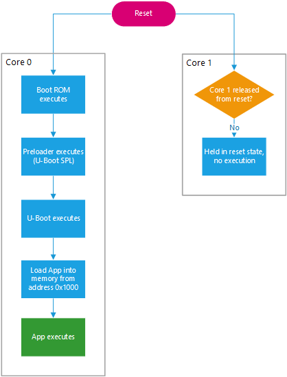
Let's have a look at the boot flow which uses U-Boot as the bootloader (note, for simplicity some steps may be omitted or simplified):
- On powerup or reset, only core 0 is enabled, and core 1 is held in a reset state (paused)
- The HPS will remap the boot ROM (located at addresses 0xFFFD0000 - 0xFFFEBFFF) to memory address 0x0, and releases core 0 from reset
- Core 0 starts executing instructions from address 0x0 - this means boot ROM program executes
- The boot ROM program reads the BSEL switches to determine the boot source, and reads sector 0 (512 bytes) from it
- If the MBR partition signature (0x55AA) exists, it switches into MBR partition mode, else it switches into raw mode
- In partition mode, the boot ROM searches for an A2 partition, if exists, loads the preloader program at the start of the A2 partition and jumps to it
- The preloader program is U-Boot SPL in this example, and it is now executing. U-Boot SPL configures the HPS, remaps the lower memory address 0x0 (was the boot ROM program) to DDR-3 SDRAM then executes main U-Boot
- U-Boot then loads and executes the desired user application, e.g. standalone application or an OS such as Linux
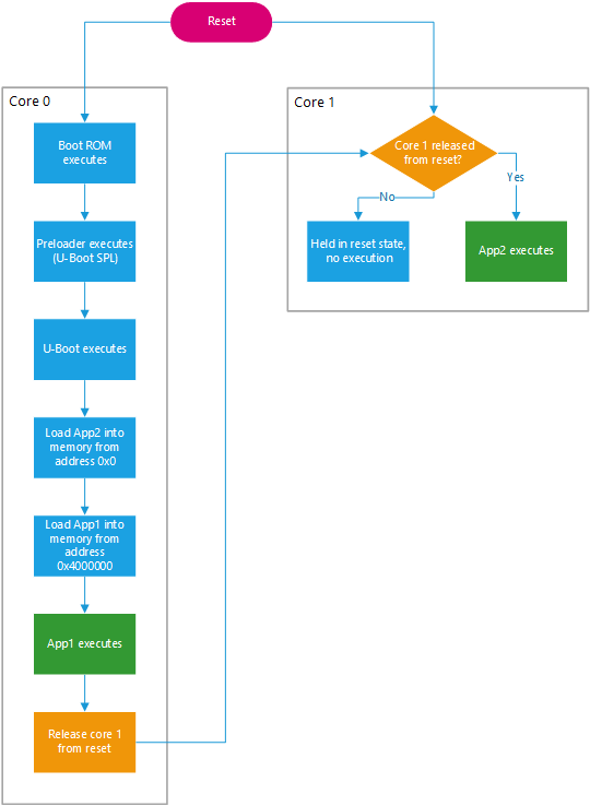
For multi-core booting, we need to change the boot flow a little bit:
In this instance, we want to run two applications concurrently, app1 to run on core 0, and app2 to run on core 1. We load both applications into memory, start app1, and have app1 release core 1 from the reset state by writing a register. When core 1 is released from reset, core 1 execution starts from address 0x0, which means the app2 we loaded earlier will execute.
Data cache coherency
In a multi-processing system, usually we want to share data or messages between the applications running on the processors (aka Inter-process communication (IPC)). This require shared data to be coherent, i.e. changes on shared data must be updated so that both cores are able to see the same data.
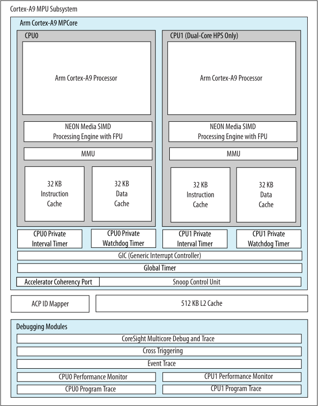
This diagram (from the Cyclone V HPS Technical Reference Manual) illustrates the different components within the cores:
The diagram shows that each core have their own MMU and L1 cache (Instruction & Data Cache) - these two components, together with the SCU and the L2 cache (if enabled) affect the data coherency between the two cores.
L1 data cache (L1 d-cache) coherency
To keep data coherent between the two cores we can apply one of these options:
- On both cores, setup MMU table with the concerned memory regions (entries) and assign attributes to enable L1 cache and set these attributes: memory_type to NORMAL and shared_type to SHARED, then enable SMP coherency support (SMP participation and MMU cache broadcasting), and enable the Snoop Control Unit (SCU)
- On both cores, setup MMU table with the concerned memory regions (entries) and assign attributes to disable L1 cache: inner_cachability_type to NON-CACHEABLE, or memory_type to DEVICE or STRONGLY ORDERED
- Disable L1 data cache
- Clean L1 data cache everytime we make a change on the shared data
Note, the SMP coherency support can be applied in an AMP system - but naturally you are required to have the MMU table set with the same memory regions and attributes on both cores.
L2 data cache coherency
The L2 cache is a separate component (ARM CoreLink Level 2 Cache Controller L2C-310), which is outside of the cores (grey coloured boxes).
Similar to L1 cache, to keep data coherent between the two cores we can apply one of these options:
- On both cores, setup MMU table with the concerned memory regions (entries) and assign attributes to enable L2 cache and set these attributes: memory_type to NORMAL and shared_type to SHARED to enable L2 caching, then enable SMP coherency support (SMP participation and MMU cache broadcasting), and enable the Snoop Control Unit (SCU)
- On both cores, setup MMU table with the concerned memory regions (entries) and assign attributes to disable the L2 cache: outer_cachability_type to NON-CACHEABLE, or memory_type to DEVICE or STRONGLY ORDERED
- Disable L2 cache
- Clean L2 cache everytime we make a change on the shared data
L1 & L2 data cache coherency for external components (e.g. FPGA IPs, F2H bridge, etc)
The SCU, ACP (Accelerator Coherency Port) and ACP ID Mapper components maintain L1 & L2 cache data coherency for AXI master peripherals that are external components to the processors, but is out of scope here.
*Note, the coherency does not support the instruction cache (L1 i-cache) because none of these components have direct access to it.
"Hello, World!" AMP example
I've made a bare-metal C, AMP version of the "Hello, World!" example, which demonstrates a basic AMP application. It consists of two separate "Hello, World!" programs, one for each of the cores. Download it from helloworld_amp.
C startup files for AMP system
I had to create my own linker files for the two cores.
Core 0 files in app1 source code:
| File | Description |
|---|---|
| bsp/tru_c5soc_ddr_core0.ld | GNU linker script |
Core 1 files in app2 source code:
| File | Description |
|---|---|
| bsp/tru_c5soc_ddr_core1.ld | GNU linker script |
Linker file settings
In an AMP system, each application should have their own memory space, which in my example is managed by the GNU linker files. You will find user settings near the beginning of linker files.
RAM size for each core
These settings configure the memory sizes for each core, i.e. application. Set them to your requirements, but ensure _CORE1_RAM_SIZE is set with the same value inside both linker files.
In app1 linker file bsp/tru_c5soc_ddr_core0.ld we have:
                            __CORE1_RAM_SIZE = 64M;

                            __CORE0_RAM_SIZE = 64M;
In app2 linker file bsp/tru_c5soc_ddr_core1.ld we have:
__CORE1_RAM_SIZE = 64M;
RAM starting address for each core
These settings do not need changing.
For core 0, the starting address is auto calculated:
__CORE0_RAM_BASE = __CORE1_RAM_BASE + __CORE1_RAM_SIZE;
For core 1, the starting address must start at 0x0, which is already preset:
__CORE1_RAM_BASE = 0x0;
Stack size for each core
Stack settings used by my startup code in both linker files:
                            __SYS_STACK_SIZE = 8192;

                            __UND_STACK_SIZE = 4096;

                            __ABT_STACK_SIZE = 4096;

                            __SVC_STACK_SIZE = 4096;

                            __IRQ_STACK_SIZE = 4096;

                            __FIQ_STACK_SIZE = 4096;
Startup
In the linker file, the ENTRY command is set to the Reset_Handler() function, which makes use of CMSIS startup files, see CMSIS/Device/c5soc/source/startup_c5soc.c.
Depending on the settings, the startup file initialises the following (note, some are conditional):
- Setup stack pointers
- Setup access permissions
- Setup vector table
- Setup NEON SIMD extension
- Setup MMU (Memory Management Unit)
- Setup L1 caches (level 1 instruction and data caches)
- Setup SMP coherency support
- Setup L2 cache
- Setup SCU (Snoop Control Unit)
- Call newlib _start() function
Note, newlib's _startup() initialises the .bss section (initialised data) and also sets up the stack pointers for us. I've overridden newlib's weak _stack_init() so that it only sets up the system and user stack pointer.
Debugging with Eclipse GDB/OpenOCD
It seems the GDB & OpenOCD plugin for "Eclipse IDE for Embedded C/C++" does not support AMP debugging, i.e. we cannot debug both cores in a single debug session. We can only debug one core at a time. If we debug on core 0, breakpoints on the other core (core 1) are ignored, they are not captured. This is same the opposite way.
I have created some Eclipse debug launch files.
| File | Description |
|---|---|
| hwamp_app1dual_debug.launch | Debugging on core 0 only. Executes both apps. |
| hwamp_app1sing_debug.launch | Debugging on core 0 only. Executes only app1 on core 0. |
| hwamp_app2dual_debug.launch | Debugging on core 1 only. Executes both apps. |
| hwamp_app2sing_debug.launch | Debugging on core 1 only. Executes only app2 on core 1. |
In the Eclipse project, app1 is set to depend on app2, but seems there is an Eclipse bug, in certain cases Eclipse will not rebuild or build app2! If you get a load or missing file error when launching a debug session, go into app2 project and rebuild it first.
Build with makefile script
Use my shortcut to start WSL and enter in this command to build the SD card image:
make sd=1
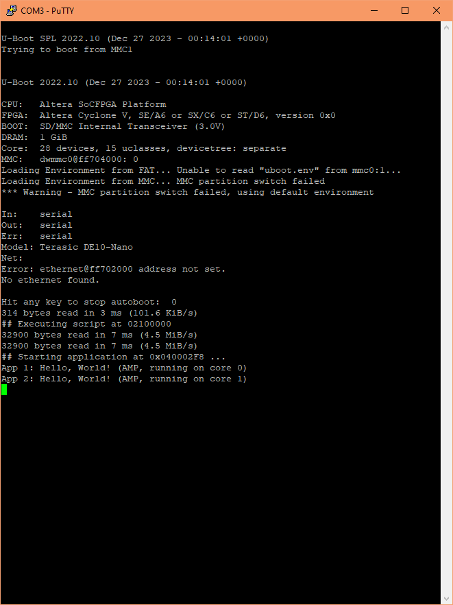
Note, it builds both projects - you should see two bin files in the console. Write the SD card image to a micro SD card and then boot it on the DE10-Nano, view the messages in a serial terminal program:
Document date: Rev 6: 13 Dec 2025 - Removed dependency on Altera HWLib and updated settings to newer tool chain
Document date: Rev 5: 07 Apr 2024 - Moved data cache coherency to a separate heading
Document date: Rev 4: 16 Mar 2024 - Corrected AXI master data coherency to L1 & L2
Document date: Rev 3: 29 Jan 2024 - Renamed linker symbols
Document date: Rev 2: 23 Jan 2024 - Correction on the L2 data coherency
Document date: Rev 1: 20 Jan 2024


