DE10-Nano: HPS and FPGA interaction - Part 1 - Ledsweep
Introduction
On the DE10-Nano board we have the Cyclone V SoC chip, it houses an FPGA and a SoC (aka HPS) system, they are separate systems and some configuration is needed for them to work together. In this guide we are going to look into that.
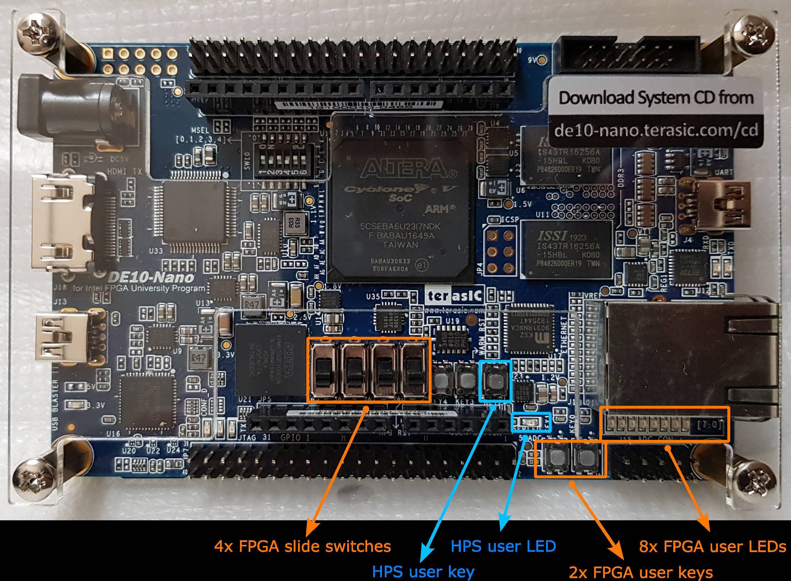
On the DE10-Nano board there are some user keys, switches and LEDs that we can utilise for this topic.
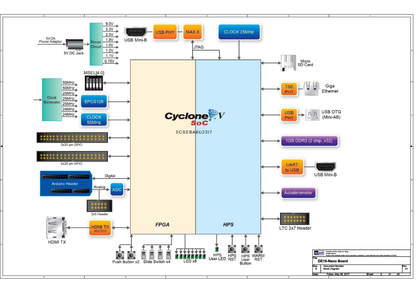
This block diagram (from the DE10-Nano schematics) illustrates where they are physically wired to:
At the bottom of the diagram we can see:
- there are 8x user LEDs, 2x user tactile keys and 4x user slide switches which are all connected to the FPGA side,
- and there are 1x user LED and 1x user tactile key which are connected to the HPS side
In part 1 of this guide we will look at an example project where the HPS is able to use the LEDs and input keys located on the FPGA side.
For the HPS to use FPGA peripherals, configuration of the FPGA logic is required to make use of the L2H or H2F bridge (data bus) which connects the two sides. The HPS is then able to read and write memory mapped registers to control the FPGA peripherals.
Peripherals on the HPS side do not require FPGA logic. Control is provided already through hardware controllers, integrated within the HPS. The HPS GPIO controller provides I/O pin control (for HPS pins) - this controller is actually an instance of the Synopsys DesignWare GPIO IP.
We will leave the HPS LED and input key for a part 2 guide.
Ledsweep
I have created a bare-metal C application and FPGA logic design that demonstrates the interaction of the two systems.
It animates the 8x FPGA LEDs by sweeping them from side to side, and pressing the FPGA tactile input keys 0 and 1 will increase and decrease the animation speed. You can download it from my github de10nano-ledsweep.
The Ledsweep consists of two separate projects:
- a Quartus Prime Lite Edition project for the FPGA hard logic design with Verilog source files
- and an Eclipse IDE for Embedded C/C++ Developers project for the HPS software with C source files
I have also made use of Arm's CMSIS 6 core library (no driver stuff) demonstrating its use in setting up the Arm Cortex-A9.
Debug the Ledsweep
For this, you will need to have the pre-requisites installed, see section 1 of Building bare-metal C programs guide for instructions.
Before we can run the application the FPGA needs to be configured (programmed) first, unfortunately we cannot automate this with Eclipse (GDB OpenOCD plugin). It does not provide the option to run a commandline script, we will have to manually run a script from outside of Eclipse, which loads a sof file to configure the FPGA.
Configuring the FPGA
- On DE10-Nano board, if there is an inserted SD card it's better to remove it (eject it) to ensure nothing boots
- Attach a USB cable between the DE10-Nano's USB Blaster II connector and your PC
- Optional: Attach a USB cable between the DE10-Nano's USB-to-serial connector and your PC
- Optional: Open a serial terminal program such as PuTTY and connect to the DE10-Nano USB-to-serial COM port
- Apply power to the DE10-Nano board
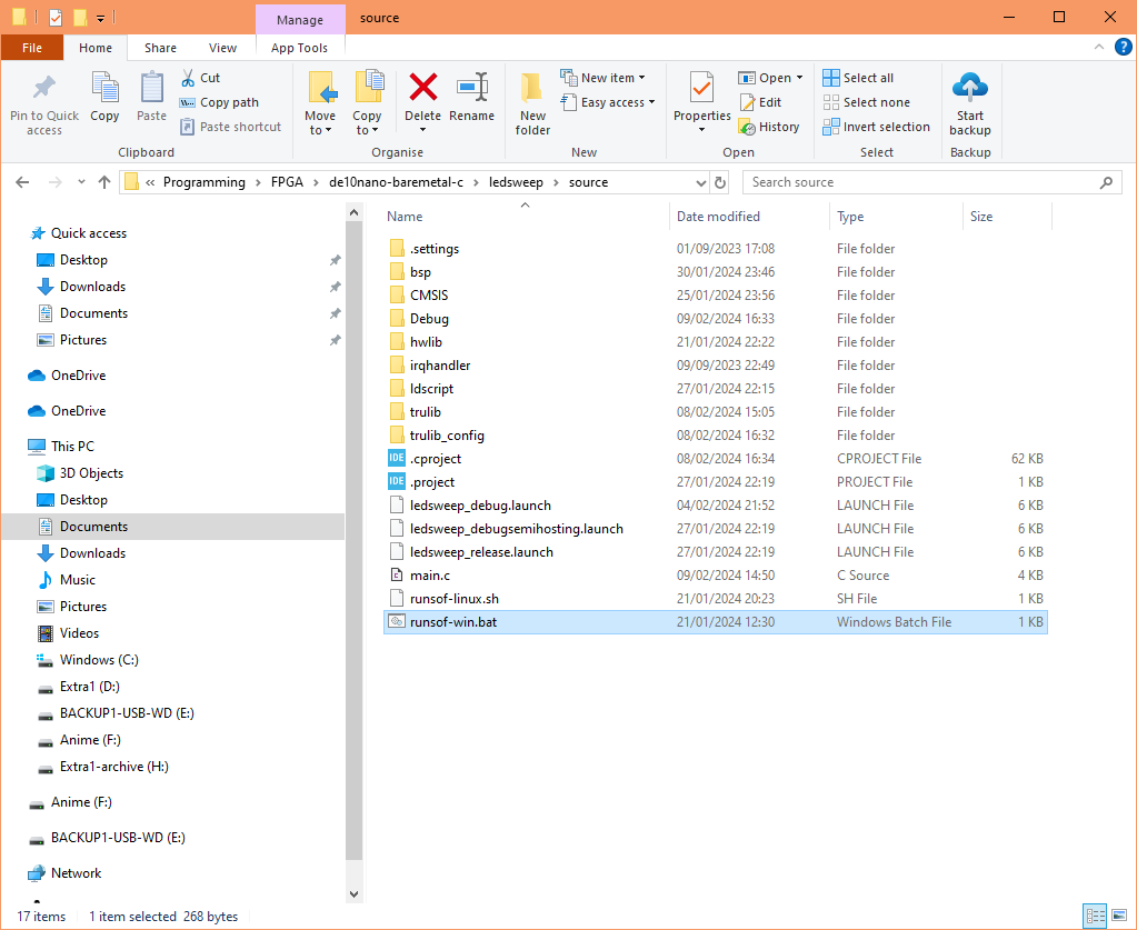
- On your PC, browse to the ledsweep source folder, there you will find my run sof scripts: runsof-win.bat and runsof-linux.sh
- On Windows double-click runsof-win.bat. On Ubuntu right-click runsof-linux.sh and select "Run as a Program"
If successful, the FPGA done orange LED should be lit on the DE10-Nano board.
Warning:
There is a bug in the latest "quartus_pgm.exe" (cli programming tool) from Quartus Prime (23.1std.0.991 for Windows). After programming, the tool may hang instead of exiting, which makes my script look bad - it stays open. You will have to close it manually.
Sometimes it does exit, but if so it will only last until a reboot or until you logout and log back into your Windows account. Hopefully, they will fix it in the next version of Quartus Prime.
Starting the HPS application in a debug session
- In Eclipse, open the project by browsing the ledsweep source folder
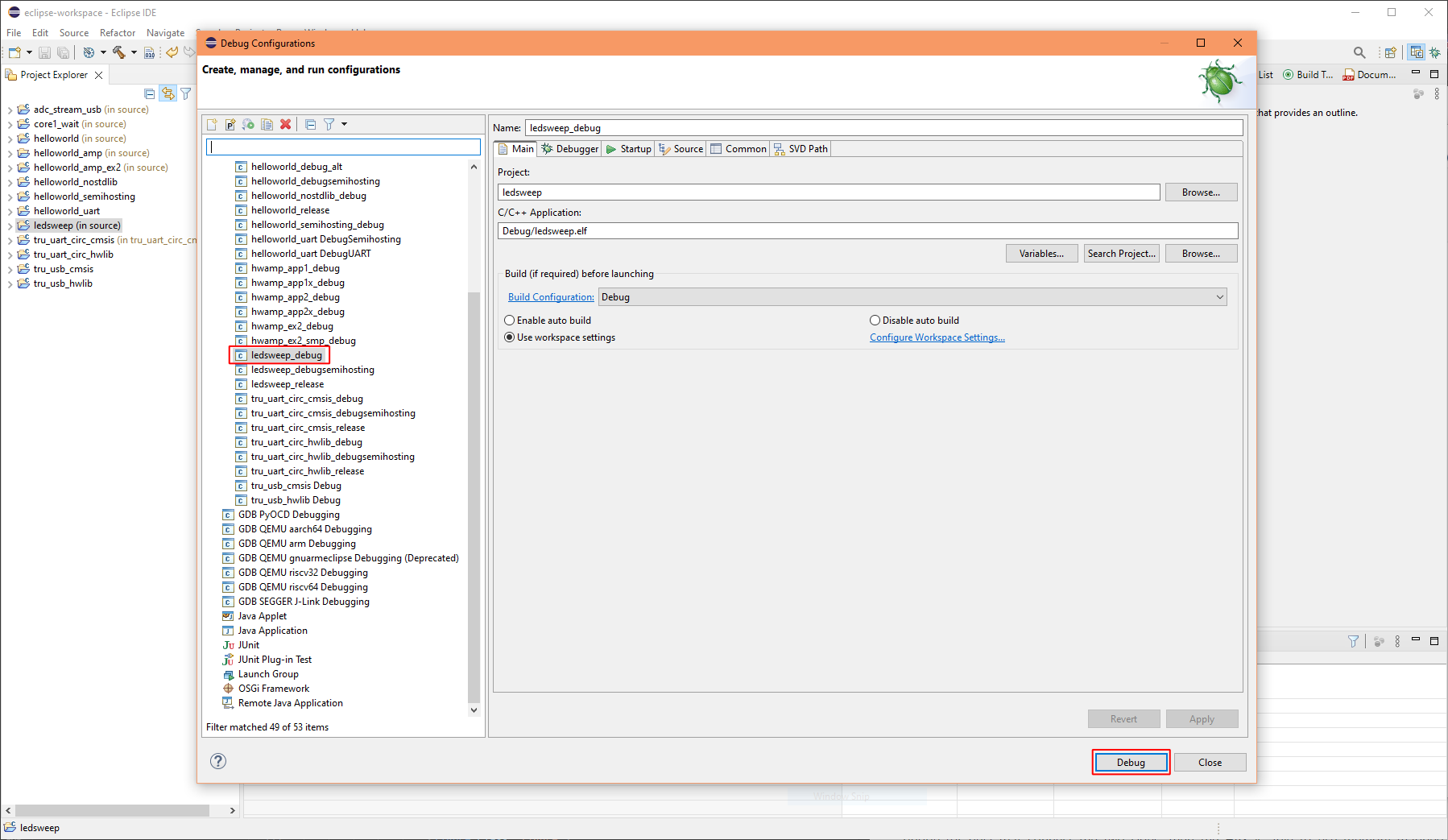
- From the menu, select Run/Debug Configurations...
- Select the ledsweep_debug debug profile
- Select the Debug button to start a debug session
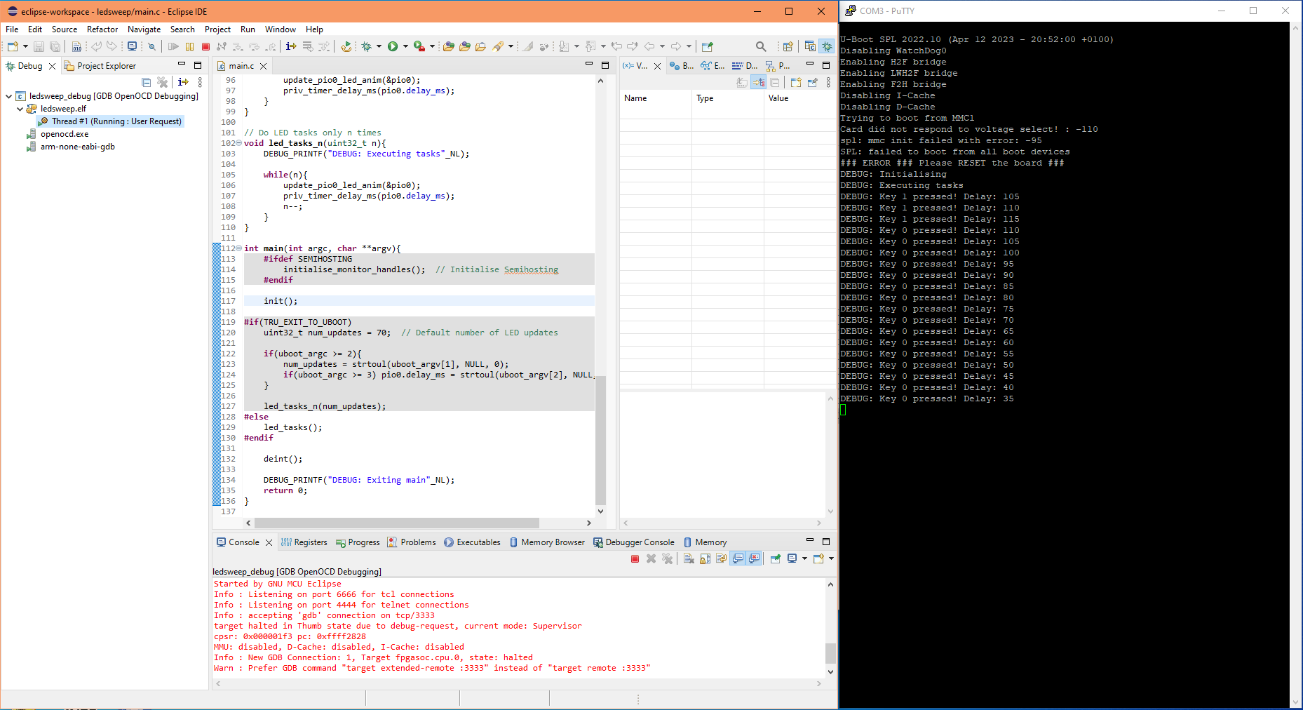
By default, execution halts at the beginning of main(), click the resume button in Eclipse to continue the execution. The LEDs should animate. Depress the tactile input key0 or key1 to trigger an interrupt, this prints a debug message in PuTTY and alters the animation speed.
Build the Ledsweep with a makefile script
For this, you will need to have the WSL2 prepared, see from 1.4 of Building the SD card image for instructions.
Use my shortcut to start WSL2 and enter in this command to build the SD card image:
make sd=1
Or, if you prefer to build the debug version which output messages to the serial terminal:
make debug sd=1
Write the SD card image to a micro SD card and then boot it on the DE10-Nano.
Application design
Overview
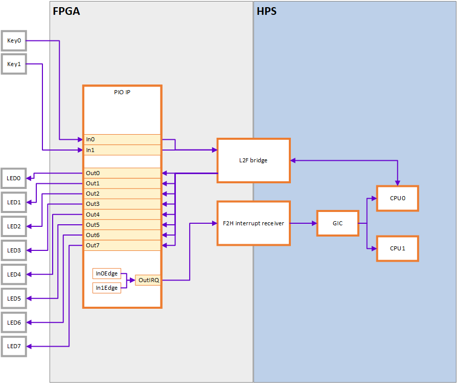
This diagram illustrates an overview of the ledsweep design (CPU1 is just for completeness, it is unused):
Bridge
The L2F bridge (data bus) enables the LEDs and inputs to be shared between the two sides.
Interrupt forwarding
The F2H interrupt receiver enables forwarding of FPGA interrupts to the GIC on the HPS side.
IO pins to bridge
In Platform Designer, the PIO IP component was added because it is the easiest method to map the L2H bridge with IO logic ports, making it easy to wire the FPGA LEDs and inputs (essentially IO pins). Note, this is not the only way of using the bridge, alternatively in Platform Designer we can export the AXI port signals and manually drive them ourself in the FPGA, but that involves more work.
Edge trigger mode
An input key would produce many interrupts from a single press, using edge trigger mode can prevent this. Note, the GIC with F2H interrupt receiver does not directly support interrupts with edge trigger mode, a solution is provided by the PIO IP, which has its own input edge capturing and IRQ output logic - we can feed this to the F2H interrupt receiver.
Platform Designer
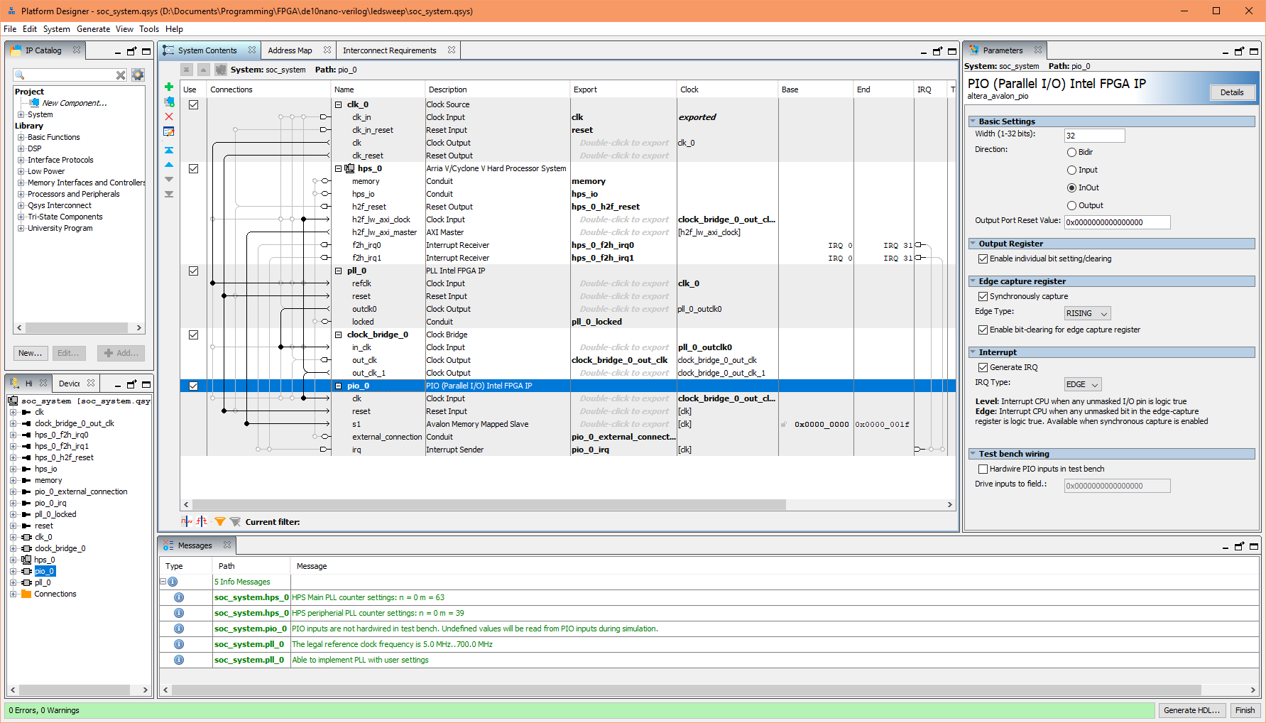
The HPS and some components in the Ledsweep hardware design are configured with the Platform Designer (a tool within Quartus Prime):
The components:
- A clock component (clk_0) which represents the main DE10-Nano onboard 50MHz clock.
- A HPS component (hps_0) which represents the HPS. We enabled the L2F bridge (set to 32-bits) and the F2H interrupt receiver (turned on Enable FPGA-to-HPS Interrupts).
- A PLL component (pio_0) for creating an 80MHz clock from the 50MHz main clock. This is for the L2H bridge and the PIO.
- A clock bridge component (clock_bridge_0) for distributing the 80MHz clock. Although, it is not actually used, it enables us to export the 80MHz clock for the FPGA to use.
- A PIO component (pio_0), a GPIO controller for mapping to a memory region of the L2F bridge. InOut mode is the easiest to use. Output register is optional, but makes it easier to use. IRQ with edge type generation is enabled.
Appendix
| Acronym | Description |
|---|---|
| HPS | Hard Processor System. In the system block diagram, HPS is the block portion representing the computer system (SoC). |
| L2F bridge | Light-weight HPS-to-FPGA bridge is an AXI-3 bridge (bus), with the HPS as master (manager) and the FPGA as slave (subordinate). |
| F2H interrupt receiver | FPGA-to-HPS interrupt receiver that forward FPGA interrupts to the GIC on the HPS side. |
| GIC | Arm Generic Interrupt Controller (PL390). The Arm Cortex-A9 doesn't have its own internal IRQ mode interrupt controller, it uses this external one instead. |
Document date: Rev 1: 15 Feb 2024
